Tin in photodiode: next step to on-chip optical data transmission
Jülich, February 21, 2017 - For a long time, scientists have been looking for a suitable solution to integrate optical components on a computer chip. But silicon and germanium alone - the material basis of chip production - are hardly suitable as a light source. Jülich physicists, together with international partners, have now presented a diode that contains tin in addition to silicon and germanium to improve its optical properties. What is special about it is that since all elements belong to the fourth main group, they are fully compatible with existing silicon technology.
Optical signal paths have long been the standard for long distances because they require only a fraction of the energy needed for electrical transmission. But existing solutions are hardly suitable for moving data back and forth by optical means directly on the chip between the processor and memory or between the processor cores of a server or PC. The materials for semiconductor lasers and diodes, so-called III-V semiconductors, belong to different main chemical groups than silicon, from which computer chips are made. This results in different lattice structures, which mean that such components can only be integrated very expensively and inefficiently.
Silicon and germanium themselves, on the other hand, belong to the so-called indirect semiconductors. Due to the energetic states of the electrons, which are possible in quantum physics, they are hardly able to emit or absorb light -- or more precisely: photons. The addition of tin changes the electronic properties of the crystal. The resulting compound becomes a direct semiconductor that can absorb and emit photons directly -- and therefore very efficiently.

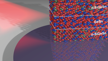
Because tin, like silicon and germanium, belongs to the fourth main group of the periodic table, the silicon-germanium-tin diode, or SiGeSn diode for short, can be applied directly to silicon in the course of chip production. The scientists fabricated the SiGeSn diode from a GeSn/SiGeSn layer system, as they explain in the journal Small. The sandwich design increases the efficiency with which the injected current is converted into light, they demonstrate in the journal Optica. By gradually changing the silicon and tin content, the researchers also succeeded in adjusting the optical wavelength within a range of 2 to 2.6 micrometers.
With the diode development, the researchers from the Peter Grünberg Institute (PGI-9) at Forschungszentrum Jülich are one step closer to developing an infrared light source for on-chip data transmission. In addition, the material could enable further applications such as photodetectors. Back in January 2015, the Jülich physicists had demonstrated the basic suitability of the SiGeSn compound in Nature Photonics using a laser device that can be applied directly to silicon chips. However, the laser at the time could not be excited electrically, but only optically to generate laser light. Its function was also limited to low temperatures of up to minus 183 degrees Celsius. In contrast, the SiGeSn photodiode currently being presented also functions at room temperature.
Video "Tin in the photodiode" - 2:30 Min long
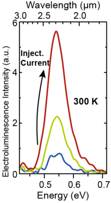
Electromagnetic spectrum of the SiGeSn diode
Electromagnetic spectrum of the SiGeSn diode at different electric current densities (red = 239 A/cm^2, yellow = 84 A/cm^2, blue = 26 A/cm^2) and 300 K (approx. 27 °C)
Original publication:
D. Stange, N. von den Driesch, D. Rainko, S. Roesgaard, I. Povstugar, J.-M. Hartmann, T. Stoica, Z. Ikonic, S. Mantl, D. Grützmacher, D. Buca
Short-wave infrared LEDs from GeSn/SiGeSn multiple quantum wells
Optica 4, 185 (2017). DOI: 10.1364/OPTICA.4.000185
N. von den Driesch, D. Stange, S. Wirths, D. Rainko, I. Povstugar, A. Savenko, U. Breuer, R. Geiger, H. Sigg, Z. Ikonic, J.-M. Hartmann, D. Grützmacher, S. Mantl, D. Buca
SiGeSn Ternaries for Efficient Group IV Heterostructure Light Emitters
Small 2017, 1603321, DOI: 10.1002/smll.201603321
Lasing in direct bandgap GeSn alloy grown on Si
S. Wirths, R. Geiger, N. von den Driesch, G. Mussler, T. Stoica, S. Mantl, Z.
Ikonic, M. Luysberg, S. Chiussi, J.M. Hartmann, H. Sigg, J.Faist, D. Buca and D. Grützmacher
Nature Photonics (2015), DOI: 10.1038/nphoton.2014.321
Further information:
Report “SiGeSn Ternaries for Efficient Group IV Heterostructure Light Emitters”
Press release on 19th January 2015 „Neuer Laser für Computerchips“
Peter Grünberg Institute, Semiconductor Nanoelectronics (PGI-9)
The research was supported by the GESNAPHOTO project (13N14159) under the "Photonics Research Germany" funding program from the German Federal Ministry of Education and Research (BMBF).
Press contact:
Tobias Schlößer
Press officer, Forschungszentrum Jülich
Tel.: 02461 61-4771
E-Mail: t.schloesser@fz-juelich.de