Team
Group leader: PD Dr. Alexander Pawlis
My team and I are interested in fabricating and studying nano-structured devices for optical quantum communication. We take a holistic approach starting with molecular beam epitaxy of heterostructures, top-down and bottom-up nano processing of the devices, to electrical and quantum optical characterization of the prototypes.
Scientific Staff
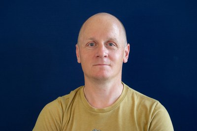
My task is the supervision of the PL laboratories of the institute. Within this framework, I support the work of the students, instruct them in the use of the equipment and optimize the experiments. My focus is in the field of optics and laser technology.
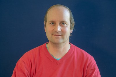
My research activity is focused on the development of highly efficient sources of indistinguishable single photons. These devices are essential components for the realization of reliable quantum computing and long-range quantum communication. In this regard, I investigate isolated impurity states in epitaxially grown semiconductor nanostructures that possess important radiative features such as distinct emission wavelength of single photons with a very short radiative lifetime.
I am involved in the development and optimization of different semiconductor systems for novel devices in the field of quantum communication. Specifically, I use molecular beam epitaxy (MBE) to grow and combine several III-V and II-VI compound semiconductors such as (Al)GaAs and Zn(Mg,Cd)Se and to understand their properties.
Technical Staff
As the technician of the Nanocluster I am responsible for the whole UHV cluster tool and the lab safety. My focus is to keep everything running so the scientist can focus on their growth experiments.
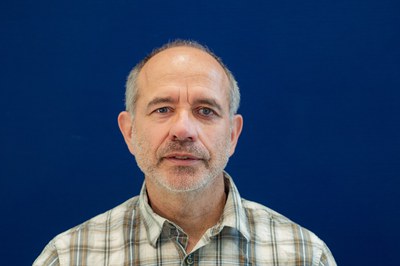
My responsibilities include technical support of the nanocluster, fabrication of semiconductor layers on the III/V MBE's and of contact layers in the Balzers evaporation chamber.
PhD students
In my PhD thesis, I am working towards the realization of solid-state qubits with an optical interface in our II/VI material system. On one hand, I am investigating the quantum-optical properties of our already well-established ZnSe-based single-photon sources regarding their application as optically controlled qubits. On the other hand, we are currently developing an all-in-situ ZnSe-based FET-platform that will serve as the basis for gate defined, i.e., electrostatically controlled qubits.
Bachelor's and Master's students

In my master’s thesis I investigate the fabrication and characterization of nano-pillar single photon sources from ZnSe:Cl quantum well heterostructures. It includes developing a spectroscopic setup for resonance fluorescence measurements. By analyzing the impact of fabrication parameters, I aim to identity the most effective technique for producing high quality single-photon sources.

In my master thesis I am working on the development and fabrication of GaAs lateral PIN diodes. I utilized the shadow wall technology for the in-situ fabrication of these structures. My focus is on optimizing the manufacturing process and investigating the electrical and optical properties of the diodes.

