Low dimension devices allow pushing detection limits and provide enhanced sensitivity to the surface potential changes due to high surface-to-volume ratio that make them promising for a number of biosensing applications. Among these devices, nanowire (NWs) field-effect transistors (FETs) are emerging as key structures of modern nanoelectronics and bioelectronics. These devices have attracted attention as excellent candidates for the development of new label-free, low-noise, high-speed and ultra-sensitive biosensors. The high aspect ratio and nanoscale diameter allow improved interfacing to living cells and provide an instrument for highly sensitive and selective analysis of biological objects.
Our strategy
- To develop field effect transistors (FETs) with new functionality, which provides fast and sensitive signal transduction from biomaterials
- To focus on solutions for realizing a next generation diagnostic platform.
- To strengthen the competitive position through innovation technology
- To develop new detection approaches utilizing new parameters and quantum phenomena
Our research goals supported by RWTH innovation award 2016 [1] include:
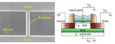
- Design and fabrication of high-performance and low-noise FETs with different sizes/geometries (Fig.1).
- Development of NW FETs with new detection principles, which provides fast and sensitive biosignal recording
- Implementation of novel thin functional layers for high-sensitive and selective detection of low concentration analyte (e.g. Troponin, CRP) or action potentials of electroactive cells (e.g. neurons, HL1 cardiac cells)
- Improvement of stability and reliability of NW FETs for biosensor applications
- Discovery and application of novel approaches and techniques for sensitivity enhancement and noise level optimization

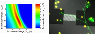
Noise spectroscopy of NW field effect transistors (FETs) allows to study transport phenomena. Our noise measurement set-up developed in-house enables us to find optimal regimes of nanochannel devices for biosensor applications. Our work includes several directions. Investigation of transport phenomena in NW FETs in order to utilize their full potential as biosensors. Improved sensitivity may be achieved by utilization of gate coupling effect (Fig.2a) and optimization of signal-to-noise ratio due to switching of scattering mechanisms [2-4]. Investigation of the conducting channel modulation effect caused by a single trap in the gate dielectric is also in focus of our studies for developing novel sensing approaches based on the single trap phenomena [5-9].

During last decade ultrathin metal nanowire structures attracted considerable attention of researchers. Ultrathin metal nanowires showed properties extremely sensitive to the surface charges, induced by the influence of molecular layers, assembled onto their surface [10]. The dynamic processes of charge transport in such systems can be analyzed using noise spectroscopy. The influence of assembled molecular layers demonstrates a response in the low-frequency noise spectra of ultrathin gold nanowires (Au NWs, ~2 nm in diameter) [11,12]. This reflect applicability of noise spectroscopy as the powerful technique to study molecular interfaces.
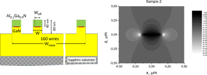
In the framework of the BMBF DIRTDANAT and Nano- and Biosystems Electromagnetic Sensing Technology (NANOBEST) projects, we are working on the exploitation of hot carrier effects and quantum phenomena in nanowire and nanotube transistor structures [13] to explore innovative applications in quantum information processing and nanotechnology (Fig.3). The main challenge is to push the sensitivity of biosensors down to the lowest analyte concentration.

In addition, a number of novel possibilities can be realized by carbon-based field-effect transistors due to effective tuning of the channel conductivity by gate electrodes and utilization of quantum effects at the nanoscale. Carbon-based nanotube (CNT) transistors are considered to be the next generation of ultra-sensitive and ultra-fast biosensing systems. We are working on development of individual CNT FETs and study their noise properties in several gate configurations with utilization of different dielectric layers and report promising results for ultra-fast biosensing applications [14]. The graphene field-effect transistors (GFETs) fabricated on a novel substrates, including flexible and biocompatible ones open new directions for very small biological signal detections [15,16].
References/Publications:
[1] RWTH innovation award 2016
[2] Highly Sensitive and Fast Detection of C-Reactive Protein and Troponin Biomarkers Using Liquidgated Single Silicon Nanowire Biosensors, Y. Kutovyi et al. MRS Advances 5, 835-846 (2020),
[3] Monitoring of Dynamic Processes during Detection of Cardiac Biomarkers Using Silicon Nanowire Field-Effect Transistors, Jie Li et al., Advanced Materials Interfaces 7, 2000508-1-11 (2020).
[4] Towards pharmacological treatment screening of cardiomyocyte cells using Si nanowire FETs, I.Zadorozhnyi et al., Biosenosrs and Bioelectronics. 137, 229-235 (2019).
[5] Amyloid-beta peptide detection via aptamer-functionalized nanowire sensors exploiting single-trap phenomena, Y.Kutovyi et al. Biosensors and bioelectronics 154, 112053-1-8 (2020)
[6] Noise suppression beyond the thermal limit with nanotransistor biosensors, Y.Kutovyi, I et al. Scientific reports. 10(1), 12678-1-11 (2020)
[7] Characteristic Frequencies and Times, Signal-to-Noise Ratio and Light Illumination Studies in Nanowire FET Biosensors, S.Vitusevich, 2020 IEEE Ukrainian Microwave Week (UkrMW), 580-585 (2020)
[8] Single-trap phenomena stochastic switching for noise suppression in nanowire FET biosensors, Y. Kutovyi et al. Japanese Journal of Applied Physics, V.60, N.SB, SBBG03-1-5 (2021)
[9] Boosting the Performance of Liquid-Gated Nanotransistor Biosensors Using Single-Trap Phenomena, Y. Kutovyi etal. Advanced Electronic Materials (2021).
[10] Activation–relaxation processes and related effects in quantum conductance of molecular junctions, F.Gasparyan et al. Nanotechnology, 31, N.4, 045001-1-7 (2020).
[11] V. Handziuk et al. J. Stat. Mech. Theory Exp., 5, 054023-1-8 (2016).
[12] Noise spectroscopy of tunable nanoconstrictions: molecule-free and molecule-modified, V. Handziuk et al. Nanotechnology 29, 385704-1-12 (2018)
[13] Interaction of sub-terahertz radiation with low-doped grating-based AlGaN/GaN plasmonic structures. Time-domain spectroscopy measurements and electrodynamic modeling, V.V. Korotyeyev et al.. Semiconductor Physics, Quantum Electronics and Optoelectronics. 22, 237-251 (2019).
[14] Noise spectroscopy to study the 1D electron transport properties in InAs nanowires, M.Petrychuk et al. Nanotechnology, 30, 30501-1-9 (2019).
[15] Graphene Nanoplatelet–Au Nanoparticle Hybrid as a Capacitive-Metal–Oxide–Semiconductor pH Sensor, A. Medhat et al. ACS Applied Electronic Materials. 3, 430-436 (2021)
[16] D.Kireev et al. Graphene field effect transistors for in‐vitro and ex‐vivo Recordings, submitted to “ IEEE transactions of Nanotechnology” (2016)
Patents:
S.Vitusevich, J.Li, S.Pud. « Device and method for measuring small voltages and potentials on a biological, chemical or other sample » . EP3066459, registered on 28.11.2018, Nr.6441336 on 30.11.2018 in Japan, Nr.ZL.201480061367.9 on 10.12.2019 in China, Nr.10,859,529 on 08.12.2020 in USA.
