Topological insulators: layering instead of mixing
Jülich, 17. November 2015 – Jülich-Aachener research team improves energy efficiency of topological insulators
Excessive heating of computer chips is a major obstacle to the development of faster and more powerful computers and cell phones. A class of materials discovered only a few years ago promises a remedy: topological insulators that conduct electricity with lower resistance and less heat generation than conventional materials. Research on this is still at the basic stage. A team from Jülich and Aachen has now found a way to tune the desired conduction properties of such materials more precisely and reliably than was previously possible. The results have been published in the current issue of the journal Nature Communications (DOI: 10.1038/ncomms9816).
So-called "topological" materials have different physical properties on their surfaces than on the inside. Topological insulators are practically insulators on the inside of the material, but on their surfaces and edges they conduct electric current almost like on rails: faster, with lower resistance and less heat generation than conventional materials. In addition, the rails act as one-way streets for electrons. The intrinsic angular momentum of the electrons - known as spin - determines the direction in which the electrons can flow. This material property is also useful for information processing and could enable the development of new spintronic devices.
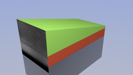
Researchers at the Peter Grünberg Institute in Jülich and RWTH Aachen University have now shown how the conductivity and energy requirements of these materials can be optimized. Their recipe for success is simplified: layering instead of mixing. Prof. Detlev Grützmacher of the Peter Grünberg Institute had the crucial idea: "Instead of alloying two semiconductors of different types as usual to obtain a topological insulator, we used molecular beam epitaxy to layer the two semiconductors on top of each other, atomic layer by atomic layer, this in turn on a silicon carrier layer." Molecular beam epitaxy is a highly precise method of producing thin crystalline layers and is increasingly being used not only in research but also for the industrial production of semiconductor structures.
In this way, the researchers were able to precisely control the atomic composition, which they documented with ultrahigh-resolution electron microscopy. "The perfect atomic composition of topological insulators is quite crucial for the electronic properties and thus energy efficiency, but is difficult to control in alloys," explains Dr. Lukasz Plucinski of the Peter Grünberg Institute.
The researchers found out which layer thicknesses are associated with optimal conduction properties using the technique of angle-resolved photoemission spectroscopy. In this technique, samples are bombarded with photons that release electrons from the material. Their energy and exit angle are measured, providing information about the energy and distribution of electrons on the surface of the sample.
Topological insulators can also, in principle, be created in semiconductor alloys and other materials using external electric fields. In the sandwich method, which the scientists jointly developed as part of the Jülich Aachen Research Alliance, section "Future Information Technology", this technical effort is unnecessary and the substrate material silicon simplifies subsequent integration in applications.
In the Virtual Institute for Topological Insulators (VITI), coordinated by the Peter Grünberg Institute at Jülich, scientists are also exploring further potential uses of the new material in basic research. For example, it could enable the detection of new quantum phenomena that have so far only been predicted theoretically, such as quasiparticles of electrons and conduction holes that form a so-called topological exciton condensate.
Original publication:
Realization of a vertical topological p-n junction in epitaxial Sb2Te3/Bi2Te3 heterostructures;
Markus Eschbach, Ewa Mlynczak, Jens Kellner, Jörn Kampmeier, Martin Lanius, Elmar Neumann, Christian Weyrich, Mathias Gehlmann, Pika Gospodaric, Sven Döring, Gregor Mussler, Nataliya Demarina, Martina Luysberg, Gustav Bihlmayer, Thomas Schäpers, Lukasz Plucinski, Stefan Blügel, Markus Morgenstern, Claus M. Schneider, Detlev Grützmacher;
Nature Communications (2015), DOI: 10.1038/ncomms9816
Further information:
Forschungszentrum Jülich
Pressemitteilung vom 29.2.2012 "Schienen für elektrischen Strom"
Pressemitteilung vom 18.8.2011 "Blick in bisher ungeahnte Tiefen"
Pressemitteilung vom 12.2.2009: "Science: Neuartiger Quanteneffekt direkt beobachtet und erklärt"
Peter Grünberg Institut – Quanten-Theorie der Materialien (PGI-1)
Peter Grünberg Institut – Theoretische Nanoelektronik (PGI-2)
Peter Grünberg Institut – Mikrostrukturforschung (PGI-5)
Peter Grünberg Institut – Elektronische Eigenschaften (PGI-6)
Peter Grünberg Institut – Halbleiter-Nanoelektronik (PGI-9)
Arbeitsgruppe Prof. Markus Morgenstern an der RWTH Aachen, II. Physikalisches Institut B
Jülich Aachen Research Alliance, Sektion FIT (Fundamentals of Future Information Technology)
Contact:
Dr. Lukasz Plucinski, Forschungszentrum Jülich, Elektronische Eigenschaften (PGI-6), Tel. 02461 61-6684
E-Mail: l.plucinski@fz-juelich.de
Prof. Dr. Detlev Grützmacher, Forschungszentrum Jülich, Halbleiter-Nanoelektronik (PGI-9), Tel. 02461 61-2340
E-Mail: d.gruetzmacher@fz-juelich.de
Dr. Gustav Bihlmayer, Forschungszentrum Jülich, Quanten-Theorie der Materialien (PGI-1), Tel. 02461 61-4677
E-Mail: g.bihlmayer@fz-juelich.de
Prof. Dr. Markus Morgenstern, RWTH Aachen, II. Physikalisches Institut B, Tel. 0241 80-27076
E-Mail: mmorgens@physik.rwth-aachen.de
Press contact:
Angela Wenzik, Scientific journalist,
Forschungszentrum Jülich,
Tel. 02461 61-6048,
E-Mail: a.wenzik@fz-juelich.de