PGI Kolloquium:Prof. Dr. Ute A. Kaiser,Materialwissenschaftliche Elektronenmikroskopie, Universität Ulm
PGI Lecture Hall, Building 04.8, 2nd floor, Room 365
Properties of low-dimensional materials obtained from experiments in a low-voltage aberration-corrected TEM
In this lecture, we report on the structural and electronic properties of low-dimensional beam-sensitive objects obtained by analytical low-voltage aberration-corrected transmission electron microscopy. Results need to be confirmed by image calculation, for high-resolution TEM images respectively for energy-filtered images of low-Z materials at low voltages, the contribution of inelastic scattering must be taken into consideration. The contributions of elastic and inelastic scattering to the image intensity cannot be separated from each other because the inelastic scattering amplitudes are influenced by elastic scattering, and vice versa. As signal-to-noise is limited for beam-sensitive materials, we show an approach to work with noisy images, to sandwich beam-sensitive objects in-between two graphene layers, and how to get the surface of graphene clean.
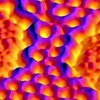
Basic crystallographic defects and their dynamics under the electron beam will be described on the atomic level (see the figure). Moreover, on the example of amorphous carbon and amorphous silica that amorphous phases of two-dimensional materials can now be studied on the level of the single atom just from direct, atom-by-atom based analysis of high-resolution images. In addition it will be shown that the monochromatic low-energy electron beam enables the acquisition of EELS spectra with exceptionally low background noise. We determine the dispersion behaviour for π and π+σ plasmons in free-standing single-layer graphene and multilayers as benchmark experiments confirming earlier calculations.
On the other end we show that lowering the energy of the electrons down to 20kV prevents various metal clusters and molecules inside CNTs from electron-beam stimulated damage which brings us to the future prospects of low-voltage aberration-corrected TEM.
Figure: A chain of carbon atoms fabricated and imaged by an 80keV electron beam (colour-coded image).
Kontakt
Martina Luysberg
Telefon: +49 2461 61-2417
Fax: +49 2461 61-6444
E-Mail: m.luysberg@fz-juelich.de