
Loading
Surface Physics
About
Solar cells contain a multitude of interfaces, many of which will be decisive for the eventual performance and stability of the device. Thus, characterizing the chemical and physical properties of surfaces is a crucial step within solar cell characterization. The big challenge is that while surfaces are characterized, eventually interfaces matter. Thus, the characterized surface of a semiconducting film is always somewhat different from the interface that is eventually limiting the efficiency of a given solar cell. The typically used methods within the field of photovoltaics are photoelectron spectroscopy techniques such as ultraviolet photoelectron spectroscopy (UPS) and X-ray photoelectron spectroscopy (XPS) as well as different scanning probe methods (e.g. Kelvin probe force microscopy).
Research Topics
Photoelectron Spectroscopy
Device Simulations
Degradation Experiments
Automated Experimentation
Ultraviolet Photoelectron Spectroscopy and Device Physics
Because surface properties are not identical to interface properties and because error bars in the analysis of e.g. band edges via UPS are huge, we combine photoelectron spectroscopy with experiments and simulations from the toolbox of solar cell device physics. This allows us to establish a quantitative link between photoelectron spectroscopy and device performance.
Over the past years, UPS measurements have been used routinely for studies aimed at better understanding performance trends as a function of the contact and transport layer properties. In these cases, the UPS data was always complemented by device simulations as well as electrical measurements to be able to properly quantify the results and identify analysis methods for UPS that provide meaningful results. Another recent study with colleagues in Potsdam was aimed at better quantifying the origin of electrostatic selectivity in perovskite solar cells by performing layer-by-layer surface photovoltage measurements.
Understanding the effect of band offsets in perovskite solar cells: Selecting suitable charge transport layers and suppressing non-radiative recombination at interfaces with the absorber layer is vital for maximizing the efficiency of halide perovskite solar cells. In this study, high-quality perovskite thin films and devices are fabricated with different fullerene-based electron transport layers and different self-assembled monolayers as hole transport layers. Then, a comparative study of a significant variety of different electrical, optical, and photoemission-based characterization techniques is performed to quantify the properties of the solar cells, individual layers, and, importantly, the interfaces between them. In addition, the limitations and problems of the different measurements, the insights gained by combining different methods, and the different strategies for extracting information from the experimental raw data, are highlighted.
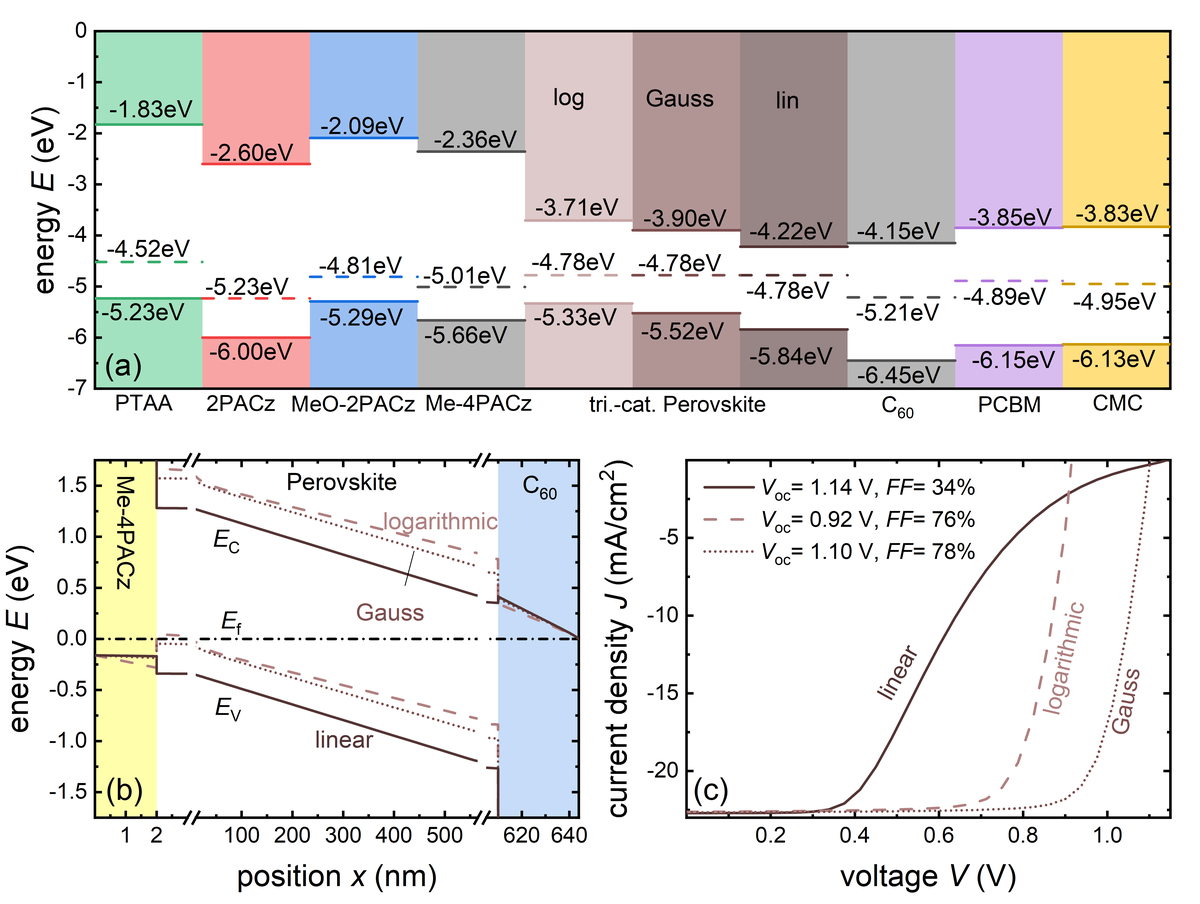
(a) Energy levels (EC, EF, EV relative to the vacuum level) for different HTLs, perovskite layers deposited on Me-4PACz, and ETLs deposited on perovskite. For all transport layers, the linear method was used to determine the EV, whereas for the perovskite, we used three methods (linear, logarithmic, and Gaussian fitting). (b) Resulting band diagrams for the stack Me-4PACz/perovskite/C60 and three fitting methods. (c) Simulated current-voltage curves showing S-shapes for the linear method (extraction barrier towards C60) and strong losses in open-circuit voltage for the logarithmic method (large band offset towards C60). Figure reproduced from under the terms of the CC-BY 4.0 license. © The authors (2023).
Team members
Research institutions / facilities
Jülich Online Semiconductor Growth Experiment for Photovoltaics (JOSEPH)
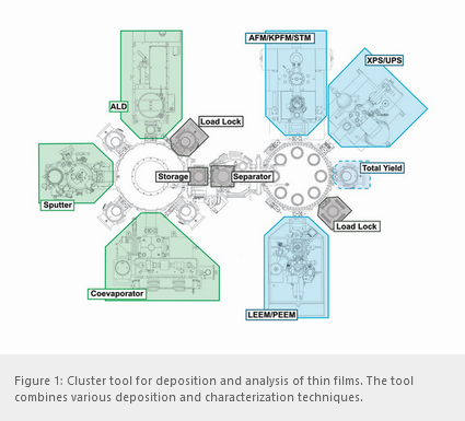
JOSEPH is a cluster tool at IMD-3. As shown in the figure below, it consists of two clusters, each with several chambers. The left cluster has several deposition chambers, including sputtering, atomic layer deposition and coevaporation. The deposition chambers are connected via a central handling system to a cluster responsible for analyzing surfaces using microscopic and spectroscopic techniques. The characterization cluster includes a surface probe measurement system (SPM) that can be used for conductive AFM measurements, scanning tunneling microscopy (STM) and Kelvin Probe Force Microscopy (KPFM) measurements. These methods allow us to measure the conductivity and work function of the surface of the deposited layers. In addition, the cluster has a UPS/XPS system that enables measurements of the work functions using UPS (ultraviolet photoemission spectroscopy) and the chemical composition using XPS (X-ray photoemission spectroscopy). With the LEEM/PEEM system, the user can investigate various properties of surfaces with high spatial resolution and simultaneously perform spectroscopic measurements. The PEEM system, for example, illuminates the layer with ultraviolet light and then generates an image of the emitted electrons, which can be spectrally filtered.
Publications
Last Modified: 09.04.2026