
Loading
Silicon Heterojunction Solar Cells
About
Silicon heterojunction (SHJ) solar cells represent a new generation of solar cells based on crystalline silicon, with which very high efficiencies can be achieved. The IMD-3 is involved in material and process development of the various thin films in solar cells, both for SHJ single junction cells and in combination with perovskites in perovskite-SHJ tandem solar cells. The development and existing infrastructure range from the wet chemical pretreatment of crystalline silicon substrates, the deposition of various functional thin films using, for example, plasma-assisted chemical vapor deposition or sputtering, to various methods of post-treatment of the layers. The process development is accompanied by a wide range of optical, electrical and microstructural characterisation methods in order to resolve the smallest changes in material behaviour and correlate them with the solar cell performance.
Research Topics
The research topics cover the complete process development of SHJ solar cells on an industrial scale. The focus is on maximising the efficiency of the solar cell, while also considering the reduction of critical, expensive or rare materials. Wet chemical processes are being optimised and adapted, various dopants and alloys for the functional thin films are being investigated, and novel contacts and thin film stacks are being researched. The aim is to establish correlations between the microstructural properties of the individual thin films and the performance of the solar cell as a whole.
Introduction

The silicon heterojunction solar cell (SHJ) represents a new generation of silicon wafer solar cells with which high levels of efficiency can be achieved. A cross-sectional structure of a SHJ solar cell is shown in Fig. 1. The IMD-3 deals with material, process, cell, module and system development for the SHJ solar cell and its applications, which covers the entire value chain of SHJ technology. Cell technology ranges from the wet chemical pretreatment of crystalline silicon wafers to the deposition of functional thin layers using various deposition processes to the final thermal treatment after deposition.
The focus of process development is on the development of cost-effective processes for the production of industrial SHJ solar cells on large-scale systems. Material development focuses on the production and characterization of silicon alloys and their implementation in SHJ solar cells. Module development specializes in lightweight and flexible SHJ modules for special applications such as vehicle-integrated photovoltaics. System research deals with life cycle assessment and cost analyzes for SHJ based PV systems such as the integration of SHJ modules in road traffic.
Further fields of work are the development of perovskite silicon tandem solar cells, SHJ solar cells in the back-contacted configuration (Interdigitated Back-Contacted: IBC), the 3D optical-electrical Simulation of SHJ solar cells, and the production and characterization of passivated SiO2 / poly-Si Contacts.
Solar Cell Development
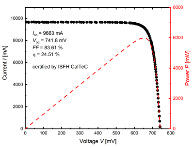
We operate a baseline that covers the entire process technology for the industrial production of high-efficiency SHJ solar cells on M2 wafer size: from wet chemical pretreatment to thin film deposition and metallization. In addition, various measurement facilities are available for characterizing the finished solar cells and the respective layers. We achieved a champion efficiency of 24.51% on M2 size (156.75 mm x 156.75 mm) wafer, which was independently certified by ISFH CalTeC (see Fig. 2).
Advanced research development based on SHJ solar cells to further increase the efficiency is also being conducted, with both scientific and industrial application perspectives. The topics are:
- Highly transparent and conductive hydrogenated nanocrystalline silicon oxide (nc-SiOx:H) as a low-parasitic absorbing window layer in SHJ solar cells
- Development of high-quality TCOs for SHJ solar cells, as alternative to indium tin oxide (ITO), with high carrier mobility and relatively low carrier density, such as ITiO and IWO, or sputtered indium-free AZO and PECVD processed doped-ZnO films, with lower costs
- Light soaking mechanism for SHJ solar cells and modules
- Long-term stability based on TCO optimization for SHJ solar cells and modules
- Catalytic doping of silicon thin films for the application in SHJ solar cells
- SHJ solar cells for the application as bottom cells in high-efficiency multi-junction solar cells, e.g. perovskite/SHJ tandem solar cells
Silicon carbide based transparent passivating contacts solar cells
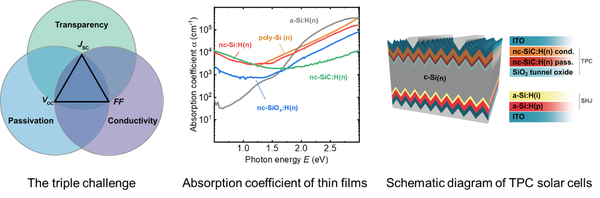
The classical triple challenge for front contacts of crystalline silicon (c-Si) solar cells - high conductivity, excellent surface passivation, and high optical transparency - are often in conflict and require compromises. For example, separating the metal contacts from the c-Si absorber with different types of passivating front contact schemes enables excellent surface passivation and accordingly high open-circuit voltages (Voc), but the solar cells often suffer from significant parasitic light absorption in the amorphous or polycrystalline silicon contact layers, leading to a significant reduction in short-circuit current density (Jsc).
A highly transparent passivating contact (TPC) offers the opportunity to solve this challenge. It consists of a wet-chemically grown thin silicon oxide followed by a bilayer stack of hydrogenated nanocrystalline silicon carbide (nc-SiC:H(n)) deposited by hot-wire chemical vapor deposition (HWCVD) and a sputtered indium tin oxide (c-Si(n)/SiO2/nc-SiC:H(n)/ITO), which combines high optical transparency and low surface recombination with a much lower need for compromise. Additionally, this contact avoids the need for additional hydrogenation or high-temperature post-deposition annealing steps. The efficient solar cell yields a high Jsc > 40 mA/cm2, and a Voc > 725 mV. While the high bandgap of nc-SiC:H(n) provides high optical transparency, the double layer structure is the key innovation leading to a combination of good passivation and high conductivity, as evidenced by the high fill factor (FF > 80%) leading to a certified efficiency of 24%.
Further tasks include upscaling the current 20 mm x 20 mm size to M2 size, developing TPC-based TCO-free solar cells, and the development of high-temperature stable TPC solar cells for industrial application.
Team members
Research institutions / facilities
Baseline for Silicon Heterojunction Solar Cells
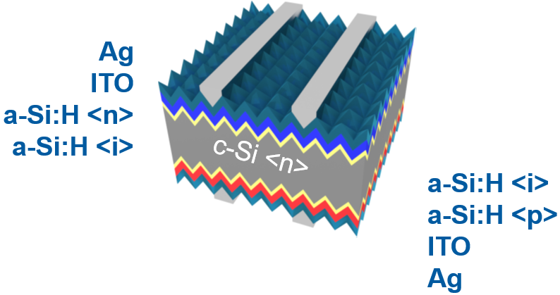
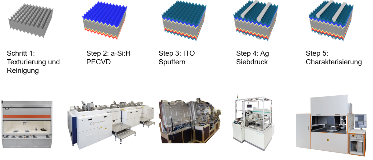
Silicon heterojunction solar cells, or SHJ solar cells for short, are solar cells that contain very thin amorphous silicon layers in addition to crystalline silicon layers (Fig. 1). These amorphous layers provide excellent passivation of the surfaces and thus enable high efficiencies. In addition, these solar cells have an advantageous temperature coefficient of rel. > -0.3 %/K and thus exhibit much better temperature behavior than conventional crystalline silicon solar cells. However, SHJ solar cells are not only convincing due to their performance, but also due to the low manufacturing effort. Only four process steps are required to manufacture SHJ solar cells (Fig. 2.). This means that production is much leaner than, for example, with the currently predominant PERC solar cells.
The Institute of Energy Materials and Devices 3 - Photovoltaics - at Forschungszentrum Jülich (IMD-3) operates a baseline that covers the entire process technology for the industrial production of high-efficiency SHJ solar cells on M2 wafer size: from wet chemical pretreatment to thin film deposition and metallization. In addition, various measurement facilities are available for characterizing the finished solar cells and the respective layers.
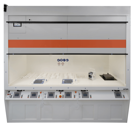
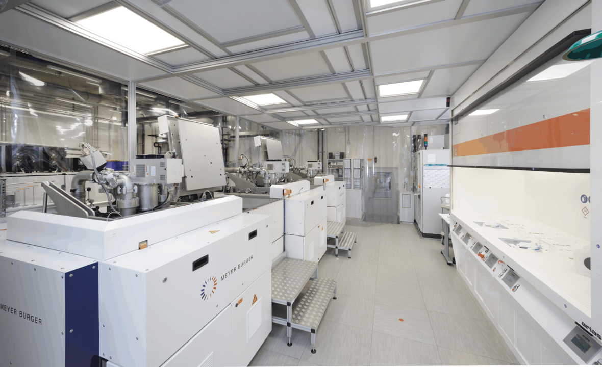
In the first process step, work is carried out on a wet bench from Arias (Fig. 3). The wet bench has five process basins and two rinsing basins in which different work steps such as saw damage removal, texturing, ozone cleaning, oxidation, removal of the oxide and rinsing by means of Quick Dump Rinse can be carried out. The basins can each accommodate a holder with 25 M2 wafers. Since the work or transport between the process steps is particle critical, it takes place in an Ionstatex clean room of class 5 or better (Fig. 4).
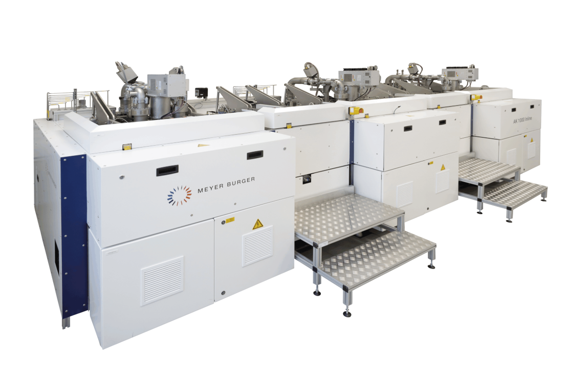
Subsequently, the various silicon layers are deposited on the wafers. Intrinsic and doped amorphous and nanocrystalline silicon layers as well as silicon oxide layers are deposited by plasma-enhanced chemical vapor deposition (PECVD) with the AK1000 from Meyer Burger (called MARIA at our institute) (Fig. 5). The system has three process chambers and two loading chambers, each of which can coat 9 M2-sized wafers. The processes are controlled in-situ by optical emission spectroscopy (OES). A throughput of 60 M2 cells per day is possible. However, other wafer sizes can also be coated.
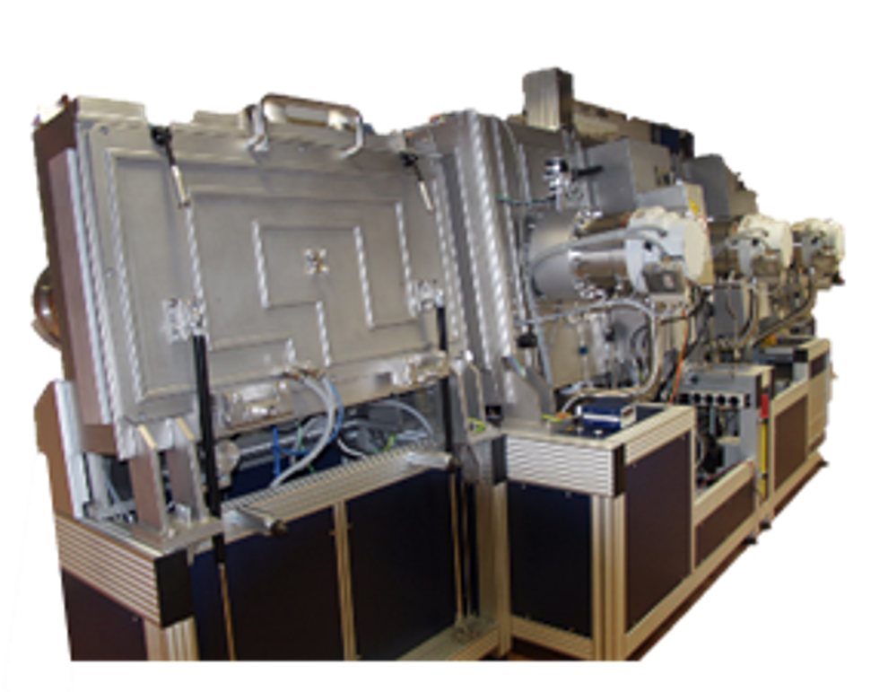
In the third process step, transparent conductive oxide (TCO) layers are deposited. In the reference process, layers of indium tin oxide (ITO) are deposited on the solar cells with the VISS 600 from Von Ardenne Anlagentechnik (Fig. 6). However, silver layers or other TCOs such as aluminum-doped zinc oxide (ZnO:Al) and indium tungsten oxide (IWO) can also be deposited with the equipment we call LISSy.
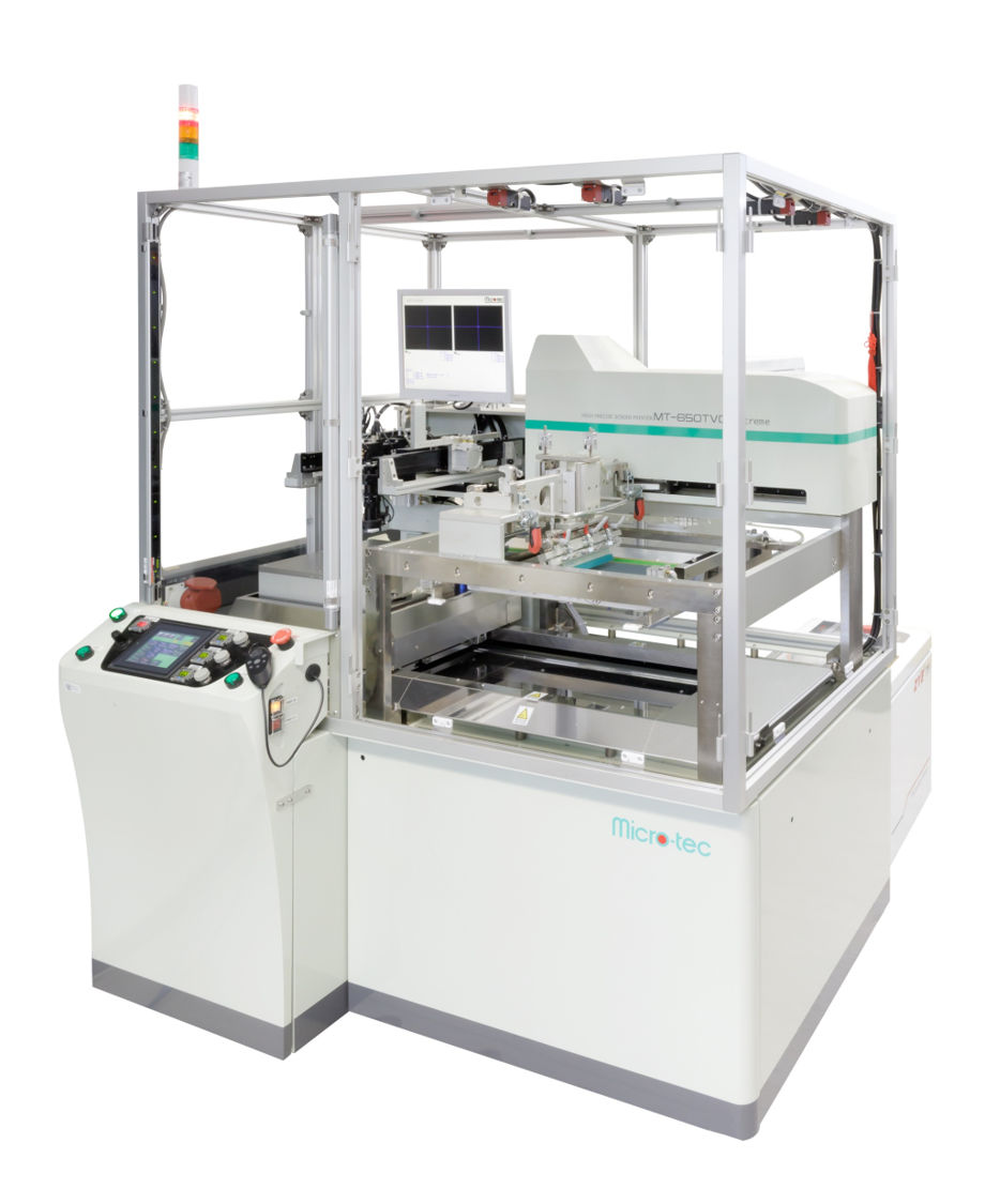
In the final process step, the metal contacts are applied to the solar cells by screen printing. The Micro-tec MT-650TVC screen printer and various screens with different numbers and widths of fingers are available (Fig. 7). Busbars can be printed subsequently on the already printed fingers (dual print). Multiple prints to reduce finger resistance are also possible thanks to precise positioning. Since the amorphous silicon layers must not be processed at high temperatures, the silver paste used is special paste for SHJ solar cells, which hardens in the oven already at 200 °C.
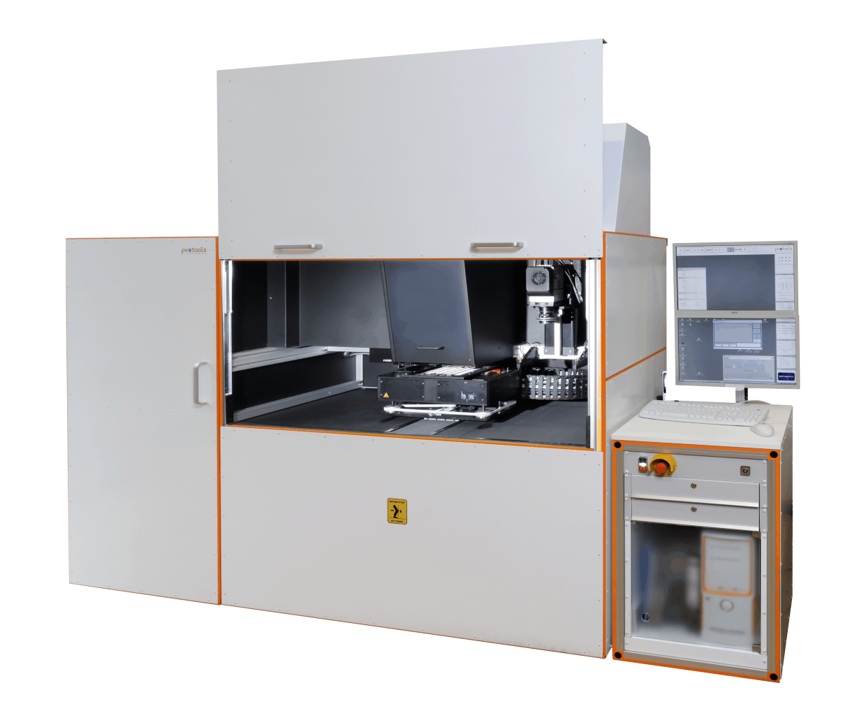
For subsequent characterization of the SHJ solar cells, the LOANA measurement facility from pv-tools with the Sinus-220 light source from Wavelabs is available (Fig. 8). Here, for example, current-voltage (IV) and external quantum efficiency (EQE) measurements are possible. For even more comprehensive analytics, a number of other measurement techniques is also available, e.g. electro-, photoluminescence, QSSPC or ellipsometry.
Publications
Recent publications
- A. Eberst, B. Xu, K. Bittkau, A. Lambertz, U. Rau, and K. Ding, "Performance improvements through gradient layers in transparent passivating contact solar cells", Cell Reports / Physical Science 6, 102658 (2025).
- B. Xu, A. Eberst, P. Fall, M. A. Yaqin, V. Lauterbach, K. Bittkau, A. Lambertz, U. Rau, and K. Ding, "Restoring sputter damage by light soaking in silicon carbide-based transparent passivating contact solar cells", Cell Reports / Physical Science 6, 102552 (2025).
- S. Alkhereibi, M. A. Yaqin, A. Eberst, B. Xu, J. Jo, H. Alsamamra, A. Lambertz, U. Rau, K. Ding, and J. Mayer, "Resolving the microstructure of aluminum-doped zinc oxide thin films grown on different silicon heterojunction solar cell structures by advanced transmission electron microscopy", Thin Solid Films 825, 140744 (2025).
Key publications
- W. Duan, A. Lambertz, K. Bittkau, D. Qiu, K. Qiu, U. Rau, and K. Ding, "A route towards high-efficiency silicon heterojunction solar cells", Prog. Photovolt. Res. Appl. 30, 384–392 (2022).
- S. Li, M. Pomaska, A. Lambertz, W. Duan, K. Bittkau, D. Qiu, Z. Yao, M. Luysberg, P. Steuter, M. Köhler, K. Qiu, R. Hong, H. Shen, F. Finger, T. Kirchartz, U. Rau, and K. Ding, "Transparent-conductive-oxide-free front contacts for high-efficiency silicon heterojunction solar cells", Joule 5, 1-13 (2021).
- M. Köhler, M. Pomaska, P. Procel, R. Santbergen, A. Zamchiy, B. Macco, A. Lambertz, W. Duan, P. Cao, B. Klingebiel, S. Li, A. Eberst, M. Luysberg, K .Qiu, O. Isabella, F. Finger, T. Kirchartz, U. Rau, and K. Ding, "A silicon carbide-based highly transparent passivating contact for crystalline silicon solar cells approaching efficiencies of 24%", Nature Energy 6, 529–537 (2021).
All publications from the group
References
Last Modified: 04.11.2025