
Loading
Optical Spectroscopy
About
Non-destructive characterization of electronic and optical properties in films, layer stacks and complete devices can be done by various types of optical spectroscopy. Optical spectroscopy primarily involves luminescence-based techniques such as transient and steady state photoluminescence. The key advantage of the techniques is their ability to do the same type of measurements on a variety of different samples (from film to cell) that include different interfaces. Thereby losses in the bulk and at interfaces can be quantified and the measurement of the charge carrier dynamics of different samples allows insights into the chemical origin of efficiency reducing defects, thereby guiding device design and optimization.
Research Topics
Transient photoluminescence
Steady-state photoluminescence
Bayesian inference
High Dynamic Range Transient Photoluminescence
An important open question in the field of halide perovskite photovoltaics is to find explanations for the high luminescence quantum yield and the long charge carrier lifetimes. We show that transient photoluminescence decays measured with a high dynamic range generally show power-law decays that lead to charge-carrier lifetimes that vary over orders of magnitude with carrier density and that may exceed hundreds of microseconds. We explain our findings by numerical models based on recombination via shallow defects that have been postulated by theory.
Further information can be found here: Yuan et al. Nature Materials 23, 391–397 (2024), https://www.nature.com/articles/s41563-023-01771-2


Mobility-Lifetime Product from Transient Photoluminescence
We developed a technique to measure both recombination and transport with a single measurement using a novel way to analyze the reabsorption of photons and in consequence the peak shift of transient photoluminescence. We measure the spectrum of the transient photoluminescence as a function of time. The spectrum shifts slightly to lower photon energies with time. The speed of this shift is indicative of how fast the electrons and holes diffuse to create a spatially homogeneous profile as a function of film depth. By comparing the peak shift as a function of time with simulations, we infer the mobility. By analyzing the decay of the overall photoluminescence as a function of time, we can infer the lifetime and product of both quantities then provides the mobility-lifetime product, a useful figure of merit for charge transport in semiconductors. An advantage of the method is that it is entirely non-destructive, does not require contacts and measures the mobility out-of-plane of the semiconductor film which is the direction of interest for photovoltaic or light emitting devices.
Further information can be found here: Yuan et al. Science Advances 11, eadt1171 (2025), https://www.science.org/doi/full/10.1126/sciadv.adt1171

Bayesian Inference
In many situations in photovoltaics, the forward problem of simulating an experiment given the material parameters is reasonably simple (software exists to do that) while the inverse problem of finding the material parameters given the experiment is extremely time consuming. This is due to the large number of unknowns (often > 10 parameters that are unknown and important) and the fact that the forward model is the numerical solution of three coupled differential equations. As one cannot invert the forward model analytically, the only traditional solution was to fit the numerical model to the data. This, however, did not allow us to quantify the confidence in the fit, identify multidimensional regions of similar fit quality in a high dimensional parameter space and to identify complementary measurements in an algorithmic way.
Bayesian inference or Bayesian parameter estimation are methods whose application to emerging photovoltaics is currently in its infancy with only a handful of publications existing. The approach that we follow is to combine neural network based surrogate models with optimization algorithms (e.g. CMA-ES [1] ) that can exploit the benefit of a high number of function evaluations that become possible by using the neural networks. The procedure is to train the neural network with >105 simulations of the forward problem (takes hours to days) and then to have the optimization algorithm use the neural network instead of the software solving the differential equations. This speeds up the optimization process per sample by about 5 orders of magnitude (around 104 parameter combinations per second can be evaluated using the neural network on a normal laptop). Thus, optimization algorithms can usually find optima in seconds to minutes and cover such a significant part of the parameter space that further statistical analysis can be performed.
We have successfully developed the method for different types of experiments (Current-voltage curves, transient photoluminescence decays) and are currently in the process of writing the first two publications on this application. An important intermediate step, especially for higher dimensional problems (many unknown material parameters), is to find suitable starting conditions for the optimization algorithm. Therefore, we develop analytical approximations that enable better starting conditions and that are based on an initial analysis of experimental data based on simple heuristics.

Interfaces for Improved Perovskite Solar Cells
The most critical interfaces within solar cells are the ones between the absorber layer and the electron and hole transport layers. Their role is to let the majority carrier pass and block the minority carrier. These interfaces often make a significant contribution to the charge-carrier selectivity of the device, ensuring that recombination losses are small, majority carrier transport is efficient and parasitic absorption is minimal. These requirements are often conflicting and lead to the challenge of finding a situation that leads to an overall performance and stability optimum.
The group holds several records in the highest open-circuit voltages, and lowest surface recombination velocities reported for certain halide perovskite compositions. The successful optimization of these interfaces was enabled primarily by the high quality of characterization techniques applied within the team as described for instance in this reference.
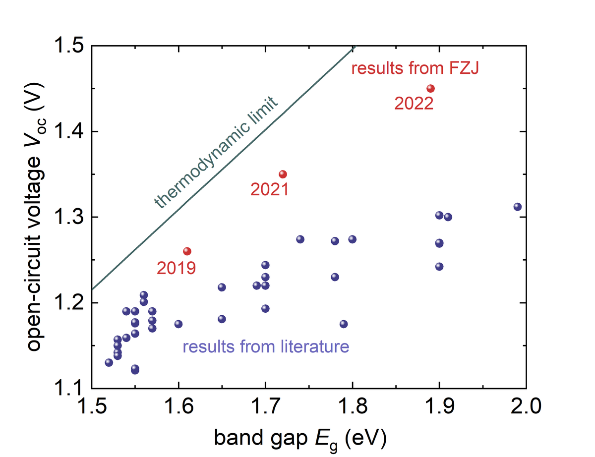
Liu et al., Open-Circuit Voltages Exceeding 1.26 V in Planar Methylammonium Lead Iodide Perovskite Solar Cells, ACS Energy Letters 2019 4 (1), 110-117 https://doi.org/10.1021/acsenergylett.8b01906
Liu et al., Interface Optimization via Fullerene Blends Enables Open-Circuit Voltages of 1.35 V in CH3NH3Pb(I0.8Br0.2)3 Solar Cells. Adv. Energy Mater. 2021, 11, 2003386. https://doi.org/10.1002/aenm.202003386
Tian et al., Quantifying the Energy Losses in CsPbI2Br Perovskite Solar Cells with an Open-Circuit Voltage of up to 1.45 V, ACS Energy Letters 2022 7 (11), 4071-4080; http://doi.org/10.1021/acsenergylett.2c01883
Team members
Research institutions / facilities
Photothermal Deflection Spectroscopy (PDS)

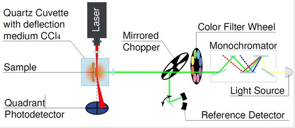
Photothermal deflection spectroscopy is based on illuminating a sample that is placed inside a cuvette filled with a liquid. The light heats up the sample and in consequence also the liquid. The liquid has to be chosen in a way that its refractive index depends on temperature. Thus, we now have a light induced temperature gradient in the liquid that can be detected by using a laser directed parallel close to the sample surface. This laser beam is then deflected by the refractive index gradient which will be detected by a photodetector. The signal detected by the photodetector is directly proportional to the amount of absorbed light and therefore to the absorptance of the sample. If the thickness is known, also the absorption coefficient (usually the parameter of interest) may be obtained with a high dynamic range of around 4 orders of magnitude.
Transient photoluminescence
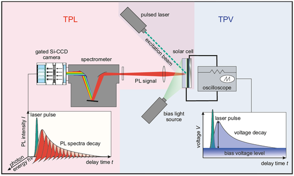
The insights obtained from transient photoluminescence (PL) measurements have contributed to an improved understanding of recombination and transport in a wide range of semiconductors. Transient photoluminescence is attractive because it allows contactless measurements of films on glass, layer stacks or complete devices while studying processes on different time- and length-scales. In particular, it permits analysis of the various recombination processes that happen in photovoltaic absorber materials and that may reduce the open-circuit voltage and subsequently the efficiency of solar cells made from these materials. However, analyzing the transients is challenging because of the multitude of (non-linear) effects that contribute to the shape of the PL transient. Recent work was focussed on combining transient photovoltage and transient photoluminescence measurements to generate an understanding of the general meaning of decay times and of the differences and similarities between electrically and optically detected transients (Krückemeier et al.,Advanced Energy Materials, 11(n/a), 2102290. doi: https://doi.org/10.1002/aenm.202102290).
Highlights
Publications
Snap view on most recent publications
Last Modified: 04.11.2025