Interfacial Electrochemistry
The interfacial electrochemistry group works with ex-situ and in-situ scanning probe techniques to characterize the interfaces of functional materials from battery and electrolysis applications. For example, topography, mechanical or electrical properties are investigated at the nanoscale to understand interfacial phenomena and subsequently improve the corresponding applications.
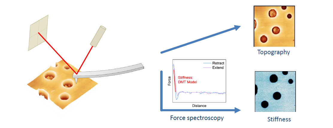
In atomic force microscopy, a tip that sits under a cantilever scans across the sample to be examined. The reflection from the laser, which is positioned on the back of the cantilever, is detected at a split photodiode. The detected laser signal is used to derive the sample topography and control the tip with accuracy to the nanometer. In addition, the tip can be pushed vertically from the sample to generate force-distance curves. From this, mechanical properties such as the stiffness of a material can also be resolved locally.
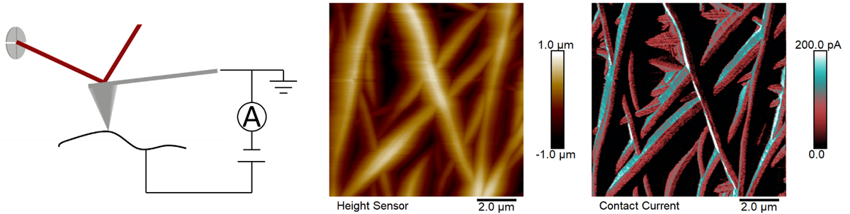
The "Height Sensor" signal shows the topography of carbon nanofibres. If a conductive tip is used and a voltage is applied to the sample, local current flows can be analysed. The simultaneously recorded "Contact Current" signal shows that current was detected at all screened carbon nanofibres and that they are conductive.

Prof. Dr. Florian Hausen
Acting Department Head
- Institute of Energy Technologies (IET)
- Fundamental Electrochemistry (IET-1)
Room R 3010