Scanning tunneling microscopy and spectroscopy
Short range ordering in ternary III-V nanowires
Stabilizing ordering instead of randomness in alloy semiconductor materials is a powerful means to change their physical properties. We used scanning tunneling and transmission electron microscopies to reveal the existence of an unrecognized ordering in ternary III-V materials.
The lazarevicite short-range order, found in the shell of InAs1-xSbx nanowires, is driven by the strong Sb-Sb repulsion along <110> atomic chains during their incorporation on unreconstructed {110} sidewalls. Its spontaneous formation under group-III-rich conditions of growth offers the prospect to broaden the limited classes of ordered structures occurring in III-V semiconductor alloys.

M. Schnedler, I. Lefebvre, T. Xu, V. Portz, G. Patriarche, J. P. Nys, S. R. Plissard, P. Caroff, M. Berthe, H. Eisele, R. E. Dunin-Borkowski, Ph. Ebert, and B. Grandidier: Lazarevicite-type short-range ordering in ternary III-V nanowires, Phys. Rev. B 94 (2016) 195306.
Quantitative description of photoexcited scanning tunneling spectroscopy and its application to the GaAs(110) surface
We have developed a quantitative description of photoexcited scanning tunneling spectra and applied to photoexcited spectra measured on p-doped nonpolar GaAs(110) surfaces. Under illumination, the experimental spectra exhibit an increase of the tunnel current at negative sample voltages only.
In order to analyze the experimental data quantitatively, the potential and charge-carrier distributions of the photoexcited tip-vacuum-semiconductor system are calculated by solving the Poisson as well as the hole and electron continuity equations by a finite-difference algorithm.
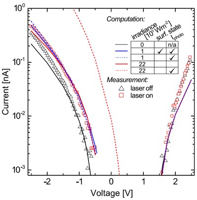
On this basis, the different contributions to the tunnel current are calculated using an extension of the model of Feenstra and Stroscio to include the light-excited carrier concentrations.
The best fit of the calculated tunnel currents to the experimental data is obtained for a tip-induced band bending, which is limited by the partial occupation of the C3 surface state by light-excited electrons.
The tunnel current at negative voltages is then composed of a valence band contribution and a photoinduced tunnel current of excited electrons in the conduction band. The quantitative description of the tunnel current developed here is generally applicable and provides a solid foundation for the quantitative interpretation of photoexcited scanning tunneling spectroscopy.
M. Schnedler, V. Portz, P. H. Weidlich, R. E. Dunin-Borkowski, and Ph. Ebert: Quantitative description of photoexcited scanning tunneling spectroscopy and its application to the GaAs(110) surface, Phys. Rev. B 91 (2015) 235305.
Importance of quantum correction for the quantitative simulation of photoexcited scanning tunneling spectra of semiconductor surfaces
Photoexcited scanning tunneling spectroscopy is a promising technique for the determination of carrier concentrations, surface photovoltages, and potentials of semiconductors with atomic spatial resolution. However, extraction of the desired quantities requires computation of the electrostatic potential induced by the proximity of the tip and the tunnel current. This calculation is based on an accurate solution of the Poisson as well as the continuity equations for the tip-vacuum-semiconductor system. For this purpose, the carrier current densities are modeled by classical drift and diffusion equations.
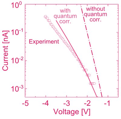
However, for small tip radii and highly doped materials, the drift and diffusion transport model significantly overestimates a semiconductor's carrier concentration near the surface, making the quantification of physical properties impossible. We apply quantum correction to the drift and diffusion model, in order to account for the so-called quantum compressibility, i.e., reduced compressibility of the carrier gas due to the Pauli principle, in the region of the tip-induced band bending. We compare carrier concentrations, potentials, and tunnel currents derived with and without quantum correction for GaN(1010) and GaAs(110) surfaces to demonstrate its necessity.
M. Schnedler, R. E. Dunin-Borkowski, and Ph. Ebert: Importance of quantum correction for the quantitative simulation of photoexcited scanning tunneling spectra of semiconductor surfaces, Phys. Rev. B 93 (2016) 195444.
Probing defect states in polycrystalline GaN grown on Si(111) by sub-bandgap laser-excited scanning tunneling spectroscopy
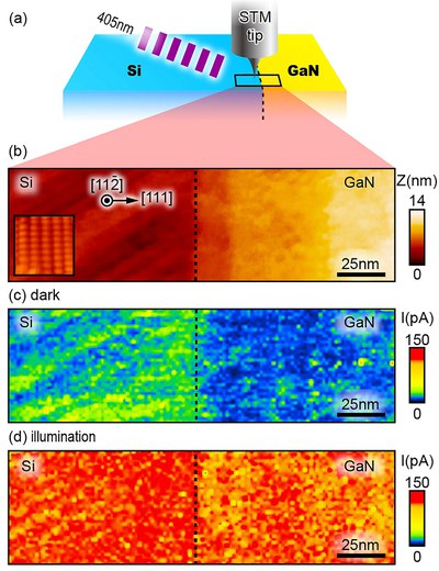
Sub-bandgap laser-excited cross-sectional scanning tunneling microscopy and spectroscopy has great potential to investigate the presence of defect states in semiconductors. The characterization method is illustrated on GaN layers grown on Si(111) substrates without intentional buffer layers.
According to high-resolution transmission electron microscopy and cathodoluminescence spectroscopy, the GaN layers consist of nanoscale wurtzite and zincblende crystallites with varying crystal orientations and hence contain high defect state densities.
In order to discriminate between band-to-band excitation and defect state excitations, we use sub-bandgap laser excitation. We probe a clear increase in the tunnel current at positive sample voltages during sub-bandgap laser illumination for the GaN layer with high defect density, but no effect is found for high quality GaN epitaxial layers. This demonstrates the excitation of free charge carriers at defect states. Thus, sub-bandgap laser-excited scanning tunneling spectroscopy is a powerful complimentary characterization tool for defect states.
F.-M. Hsiao, M. Schnedler, V. Portz, Y.-C. Huang, B.-C. Huang, M.-C. Shih, C.-W. Chang, L.-W. Tu, H. Eisele, R. E. Dunin-Borkowski, Ph. Ebert, and Y.-P. Chiu: Probing defect states in polycrystalline GaN grown on Si(111) by sub-bandgap laser-excited scanning tunneling spectroscopy, J. Appl. Phys. 121 (2017) 015701.
Intrinsic electronic properties of high-quality wurtzite InN
Recent reports suggested that InN is a highly unusual III-V semiconductor, whose behavior fundamentally differs from that of others. We therefore analyzed its intrinsic electronic properties on the highest available quality InN layers, demonstrating the absence of electron accumulation at the (1010) cleavage surface and in the bulk.
The bulk electron density is governed solely by dopants. Hence, we conclude that InN acts similarly to the other III-V semiconductors and previously reported intriguing effects are related to low crystallinity, surface decomposition, nonstoichiometry, and/or In-adlayers.

H. Eisele, J. Schuppang, M. Schnedler, M. Duchamp, C. Nenstiel, V. Portz, T. Kure, M. Bugler, A. Lenz, M. Dahne, A. Hoffmann, S. Gwo, S. Choi, J. S. Speck, R. E. Dunin-Borkowski, and Ph. Ebert: Intrinsic electronic properties of high-quality wurtzite InN, Phys. Rev. B 94 (2016) 245201.
Strain and compositional fluctuations in Al0.81In0.19N/GaN heterostructures
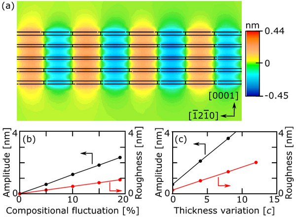
The strain and compositional fluctuations of nearly lattice-matched Al0.81In0.19N/GaN heterostructures are investigated by cross-sectional scanning tunneling microscopy and selected area electron diffraction measurements in scanning electron transmission microscopy.
The presence of strain induces height modulations governed by different roughness components at the cleavage surfaces. The surface height modulations are compatible with a relaxation of alternately compressive and tensile strained domains, indicating compositional fluctuations. Changes of the a lattice constant are traced to interface misfit edge dislocations. The dislocations induce steps increasing the roughness within the Al0.81In0.19N layers.
V. Portz, M. Schnedler, M. Duchamp, F.-M. Hsiao, H. Eisele, J.-F. Carlin, R. Butté, N. Grandjean, R. E. DuninBorkowski, and Ph. Ebert: Strain and compositional fluctuations in Al0.81In0.19N/GaN heterostructures, Appl. Phys. Lett. 109 (2016) 132102.
Fermi-level pinning and intrinsic surface states of Al1-xInxN(1010) surfaces
The electronic structure of Al1-xInxN(1010) surfaces is investigated by cross-sectional scanning tunneling spectroscopy and density functional theory calculations. The surface exhibits empty Al and/or In-derived dangling bond states, which are calculated to be within the fundamental bulk band gap for In compositions smaller than 60%.

The energy of the lowest empty In-derived surface state is extracted from the tunnel spectra for lattice-matched Al1-xInxN with In compositions of x = 0.19 and x = 0.20 to be EC − 1.82 ± 0.41 and EC − 1.80 ± 0.56 eV, respectively, in good agreement with the calculated energies. Under growth conditions, the Fermi level is hence pinned (unpinned) for In compositions smaller (larger) than 60%. The analysis of the tunnel spectra suggests an electron affinity of ~3.5 eV for nonpolar lattice-matched Al1-xInxN cleavage surfaces, which is large compared to linearly interpolated values of polar AlN and InN (0001) surfaces.
V. Portz, M. Schnedler, L. Lymperakis, J. Neugebauer, H. Eisele, J.-F. Carlin, R. Butté, N. Grandjean, R. E. Dunin-Borkowski, and Ph. Ebert: Fermi-level pinning and intrinsic surface states of Al1-xInxN(1010) surfaces, Appl. Phys. Lett. 110 (2017) 022104.
Polarity-dependent pinning of a surface state
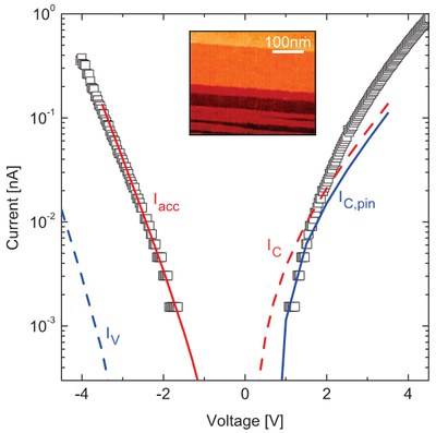
We illustrate a polarity-dependent Fermi level pinning at semiconductor surfaces with chargeable surface states within the fundamental band gap.
Scanning tunneling spectroscopy of the GaN(1010) surface shows that the intrinsic surface state within the band gap pins the Fermi energy only at positive voltages, but not at negative ones. This polarity dependence is attributed to arise from limited electron transfer from the conduction band to the surface state due to quantum mechanically prohibited direct transitions.
Thus, a chargeable intrinsic surface state in the band gap may not pin the Fermi level or only at one polarity, depending on the band to surface state transition rates.
M. Schnedler, V. Portz, H. Eisele, R. E. Dunin-Borkowski, and Ph. Ebert: Polarity-dependent pinning of a surface state, Phys. Rev. B 91 (2015) 205309.

Contact:
Dr. Philipp Ebert
Phone: +49 2461 61-5023
E-Mail: p.ebert@fz-juelich.de
