Research facilities
Jülich Online Semiconductor Growth Experiment for Photovoltaics (JOSEPH)
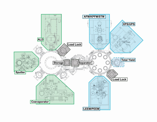
JOSEPH is a double cluster tool at IMD-3. As shown in Figure 1, it consists of two clusters with several chambers each. The left cluster provides several deposition chambers including sputtering, atomic layer deposition and coevaporation. The deposition chambers are connected through a central handling system to a cluster dedicated to the analysis of surfaces with microscopic and spectroscopic techniques. The characterization cluster includes a surface probe measurement system (SPM) that can be used for conductive AFM measurements, Scanning Tunneling Microscopy (STM) and for Kelvin-Probe Force Microscopy (KPFM) measurements. These methods allow us to measure the conductivity and the workfunction of the surface of the deposited layers. In addition, the cluster contains a UPS/XPS system that allows measurements of workfunctions via UPS (ultraviolet photoemission spectroscopy) and chemical composition via XPS (X-ray photoemission spectroscopy). The LEEM/PEEM system allows the user to study various properties of surfaces with high spatial resolution while enabling also spectroscopic measurements. The PEEM system for instance works by illuminating the layer with ultraviolet light and then generates an image of the emitted electrons that may be spectrally filtered.
Contact persons


Photothermal Deflection Spectroscopy (PDS)
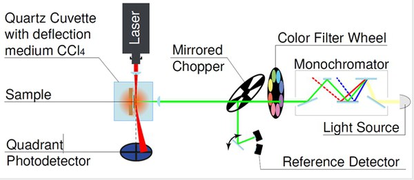
Photothermal deflection spectroscopy is based on illuminating a sample that is placed inside a cuvette filled with a liquid. The light heats up the sample and in consequence also the liquid. The liquid has to be chosen in a way that its refractive index depends on temperature. Thus, we now have a light induced temperature gradient in the liquid as shown in Fig. 2 that can be detected by using a laser directed normal to the monochromatic light used to excite the sample. This laser beam is then deflected by the refractive index gradient which will be detected by a photodetector. The signal detected by the photodetector is directly proportional to the amount of absorbed light and therefore to the absorptance of the sample. If the thickness is known, also the absorption coefficient (usually the parameter of interest) may be obtained with a high dynamic range of around 4 orders of magnitude.
Transient photoluminescence
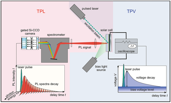
The insights obtained from transient photoluminescence (PL) measurements have contributed to an improved understanding of recombination and transport in a wide range of semiconductors. Transient photoluminescence is attractive because it allows contactless measurements of films on glass, layer stacks or complete devices while studying processes on different time- and length-scales. In particular, it permits analysis of the various recombination processes that happen in photovoltaic absorber materials and that may reduce the open-circuit voltage and subsequently the efficiency of solar cells made from these materials. However, analyzing the transients is challenging because of the multitude of (non-linear) effects that contribute to the shape of the PL transient. Recent work was focussed on combining transient photovoltage and transient photoluminescence measurements to generate an understanding of the general meaning of decay times and of the differences and similarities between electrically and optically detected transients [1].
References
[1] Krückemeier, L., Liu, Z., Krogmeier, B., Rau, U., & Kirchartz, T. (2021). Consistent Interpretation of Electrical and Optical Transients in Halide Perovskite Layers and Solar Cells. Advanced Energy Materials, 11(n/a), 2102290. doi:https://doi.org/10.1002/aenm.202102290

Last Modified: 15.07.2024