Topological Insulators: Shedding Light on Parallel Transport Channels
26 September 2018
Multi-tip STM is used to reveal detailed transport properties of thin films of the promising topological insulator (TI) material BiSbTe3. To study the electronic and transport properties of BiSbTe3 films, scientists from the PGI-3, PGI-6, and PGI-9 institutes at Forschungszentrum Jülich combined angle-resolved photoemission spectroscopy and gated four-tip scanning tunneling microscopy was conducted, gaining access to a comprehensive picture of the transport.
A model developed specifically for this analysis enabled them to disentangle the transport occurring through the different channels (the surface states channels on the top and bottom of the sample and the bulk) and to obtain the gate-dependent conductivities, charge carrier concentrations, and mobilities. This combination of experimental techniques and data analysis is of general applicability and should prove useful for studying other samples.
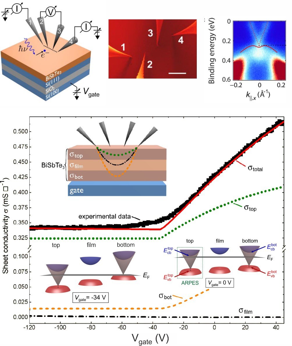
Figure caption: Top panel left: Schematic of the measurement geometry and results obtained by photoemission spectroscopy and four-probe measurements. Middle: Scanning electron microscopy image of the four-probe setup with equidistant tip spacing. Scale bar: 100 μm. Right: Photoemission intensity as a function of binding energy with the Dirac cone indicated by dotted red lines. Bottom image: Measurement of the gate-dependent TI film sheet conductivity (black squares) and fit of the transport model, as well as the individual contributions of the model. The colored lines in the inset show current paths through the individual channels. Note that the film thickness d = 10 nm is much smaller than the tip spacing of 100 μm, which are used in the transport measurement. The insets show the band schemes at different voltages.
More information can be found in
npj Quantum Materials 3, 46 (2018)
.