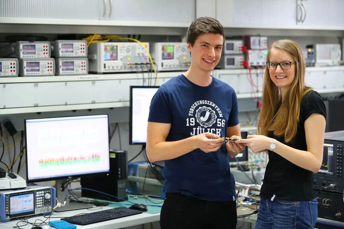
Alfonso Rafael Cabrera Galicia - DR project

On Chip Bias Circuits for Cryogenic Applications

Doctoral Researcher: Alfonso Rafael Cabrera Galicia
Local ZEA-2 Supervisor: Ashok Arun
Academic Supervisor: Stefan van Waasen, University of Duisburg-Essen (UDE)
Topic: Quantum Computing
Research Field: Information

Many scientific experiments are performed at extreme cryogenic temperatures, between 1K to 10mK, in order to fulfill essential environmental conditions for the observation and exploitation of a physical phenomenon; e.g. super conductivity or thermal noise reduction. Therefore, most of the cryogenic experiments are carry out inside dilution fridges able to reach temperatures below 1K, but with limited cooling power. This sets a limit to the amount of heat load, due to electrical power dissipation and physical mass contributions, that can be handled by the fridge.

Alfonso Rafael Cabrera Galicia's DR project
Integrated circuits in wafer

Some of these experiments are the quantum bit manipulation, the polarization of sensitive resistive bolometers and the operation of submillimeter cameras based on kinetic inductance detectors [1] [2] [3] [4]. In addition, all of these experiments require some form of control or readout system. Moreover, by implementing this system by means of an ASIC, several benefits (e.g. signal processing in situ and reduction of heat load) for the development of the cryogenic experiment could be obtained. Allowing the lightening of the fridge specifications or the inclusion of more sensors [5].

Some of the fundamental blocks of any ASIC are the bias circuits, since these provides a stable voltage or current reference to other circuit blocks. Subsequently, it is critical to develop bias circuits (e.g. bandgap references, linear and switching voltage regulators) that are capable of cryogenic operation and can satisfy the specifications imposed by the experiment. Essentially, the goal of this research project is the development of cryogenic bias circuits. To achieve it, the ZEA-2 is proposing the use of an IC technology based on UTBB FDSOI CMOS devices, which are able to operate at cryogenic temperatures [6] [7].

References

[1] Elzerman, J. M., R. Hanson, L. H. Willems van Beveren, B. Witkamp, L. M. K. Vandersypen, and L. P. Kouwenhoven. “Single-Shot Read-out of an Individual Electron Spin in a Quantum Dot.” Nature 430, no. 6998 (July 2004): 431–35. https://doi.org/10.1038/nature02693.
[2] Arute, Frank, Kunal Arya, Ryan Babbush, Dave Bacon, Joseph C. Bardin, Rami Barends, Rupak Biswas, et al.
“Quantum Supremacy Using a Programmable Superconducting Processor.” Nature 574, no. 7779 (October 2019): 505–10. https://doi.org/10.1038/s41586-019-1666-5.
[3] Broïse, Xavier de la, and Olivier Gevin.
“ECLIPSE, the Cryogenic Readout Circuit of the Polarimetric Camera BBOP for the SPICA Space Observatory Project.” Journal of Low Temperature Physics, February 1, 2020. https://doi.org/10.1007/s10909-020-02339-z.
[4] Castillo-Dominguez, E., P. Ade, P. S. Barry, T. Brien, S. Doyle, D. Ferrusca, V. Gomez-Rivera, et al. “Mexico-UK
Sub-Millimeter Camera for Astronomy.” Journal of Low Temperature Physics 193, no. 5–6 (December 2018): 1010–15. https://doi.org/10.1007/s10909-018-2018-9.
[5] B. Patra, et al., “A Scalable Cryo-CMOS 2-to-20GHz Digitally Intensive Controller for 4×32 Frequency Multiplexed
Spin Qubits/Transmons in 22nm FinFET Technology for Quantum Computers”; Proceedings of the 2020 IEEE International Solid- State Circuits Conference (ISSCC), San Francisco, CA, USA, 2020. http://isscc.org/
[6] Carter, R., J. Mazurier, L. Pirro, J-U. Sachse, P. Baars, J. Faul, C. Grass, et al. “22nm FDSOI Technology for
Emerging Mobile, Internet-of-Things, and RF Applications.” In 2016 IEEE International Electron Devices Meeting (IEDM), 2.2.1-2.2.4. San Francisco, CA, USA: IEEE, 2016. https://doi.org/10.1109/IEDM.2016.7838029.
[7] Bonen, S., U. Alakusu, Y. Duan, M. J. Gong, M. S. Dadash, L. Lucci, D. R. Daughton, et al. “Cryogenic
Characterization of 22nm FDSOI CMOS Technology for Quantum Computing ICs.” IEEE Electron Device Letters, 2018, 1–1. https://doi.org/10.1109/LED.2018.2880303.

  • Central Institute of Engineering, Electronics and Analytics (ZEA)
  • Electronic Systems (ZEA-2)
Building 02.5
02461 61 2425
E-Mail

Publications

Last Modified: 14.07.2023