Electrons on the fast track
Ballistic electrons are among the most fascinating phenomena in modern quantum materials. Unlike ordinary electrons, they do not scatter off imperfections in the material and therefore travel from A to B with almost no resistance – like a capsule in a pneumatic tube. This behaviour often occurs in confined one- or two-dimensional materials. We developed a model that can detect this distinct flow of electrons under realistic conditions.
Ballistic electron channels forming along the edges of two-dimensional topological materials are regarded as highly promising for future electronics: they could form the basis for energy-efficient circuits and quantum computers with robust qubits. The new approach builds on the theory of ballistic charge transport developed by Rolf Landauer several decades ago. However, his classical model only describes an idealized case – Landauer assumed that electrons can enter or leave such a channel only at its ends.
Our model, however, takes a decisive step further. It considers that such a ballistic charge channel does not exist in isolation but forms the edge of a likewise conductive material through which the current is injected. Electrons can therefore enter or exit along the entire length of the channel. This allows us to describe the behaviour of such edge channels for the first time in a way that reflects what actually happens in experiments. Our theory also provides distinct signatures that can be used to identify lossless, ballistic current flow and distinguish it from conventional charge transport.
The model shows that the current flow through the two-dimensional material changes fundamentally due to the presence of a ballistic channel. It predicts characteristic voltage distributions that can be directly observed with nanoscale probes or multi-tip scanning tunnelling microscopes. This makes it possible to experimentally distinguish between ballistic and dissipative – that is, lossy – currents, a crucial step towards proving the existence of these exotic conduction channels beyond doubt and harnessing them for future devices.

Recent reference
Moors, K., Wagner, C., Soltner, H., Lüpke, F., Tautz, F. S., & Voigtländer, B. (2025). Distributed current injection into a one-dimensional ballistic edge channel. Physical Review Letters. DOI: https://doi.org/10.1103/l47r-plxq
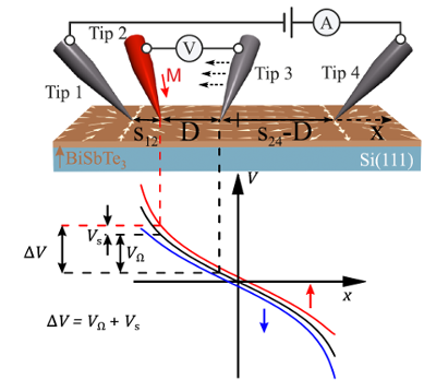
Charge transport at nanostructures of quantum materials
We reveal the nanoscale transport properties of thin films of promising quantum materials like topological insulators using multi-tip STM.
Multiple parallel conduction channels exist in topological insulator thin films. To shed light on parallel transport channels in these quantum materials (top and bottom topological surface states as well as the interior of the film) we use distance dependent and gated four-probe measurements. We obtain conductivities, charge carrier concentrations, and mobilities and can disentangle top from bottom topological surface states at thin films of BiSbTe3 [1, 2]
Moreover we have measured one of the hallmarks of topological insulators, the intrinsic spin polarisation in the topologically protected surface states, is measured at room temperature in-situ by means of four-probe scanning tunneling microscopy (STM) at a BiSbTe3 thin film [3].