Multi-tip Scanning Probe Microscopy
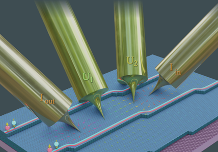
The banner image shows four tips of a multi-tip scanning probe microscope contacting a thin flake of the topological insulator BiBr for microscale electrical measurements.
About
We study the intriguing charge transport properties of quantum materials like topological insulators and novel 2D materials. For the best access to nanoscale charge transport properties, we develop novel multi-tip SPM instruments and corresponding measurement techniques.
Research Topics
- Multi-tip SPM instrument development
- Charge transport at nanostructures of quantum materials
- Charge transport at surfaces

Members

Dr. Vasily CherepanovSenior scientist at Peter Grünberg Institute (PGI-3) Building 02.4 / Room 322+49 2461/61-6636

Dr. Timofey BalashovPostdoc at Peter Grünberg Institute (PGI-3) Building 02.4w / Room 320+49 2461/61-3469

Dr. Jonathan Karl HofmannPostdoc at Peter Grünberg Institute (PGI-3) Building 02.4w / Room 126+49 2461/61-6362
Research

Recent Publications
Last Modified: 04.05.2026