Graphene
We develop new approaches to obtain high-quality graphene, grown epitaxially on silicon carbide (SiC), a wide band gap semiconductor. In particular, we try to realise wafer-size samples with unconventional twist angles.

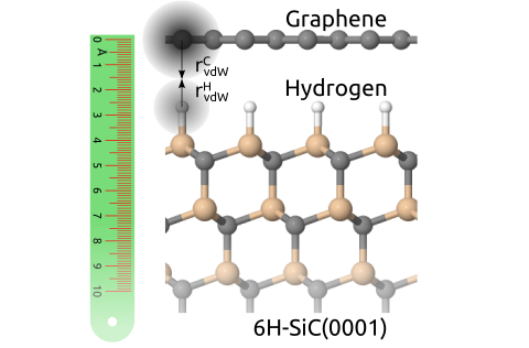
Graphene is the first 2D material that has been isolated mechanically as a layer of single-atom thickness. It shows very attractive electronic and mechanical properties [1]. It’s fingerprint is the so called Dirac cone that becomes visible in angular resolved photoemission. Another important aspect is the electronic decoupling of the graphene sheets from their support, often a metal substrate. However, for device fabrication it is necessary to grow graphene epitaxially on non-metallic substrates. SiC is an attractive substrate, because it is a wide-band gap semiconductor. We have studied the coupling of graphene to various modified SiC substrates [2, 3], as well as n- and p-doping [4, 5, 6, 7, 8]. The electronic decoupling can be proven by a suppression of electronic charge transfer through the interface, or by a precise determination of the distance between the graphene sheet and the substrate, which in turn can be measured using NIXSW. Recently, we succeeded in modifying the orientation of graphene during epitaxy in a self-limiting manner [9]. This is the basis for growing twisted bilayer graphene at specific angles epitaxially, an entry point into twistronics.