Design of the STM
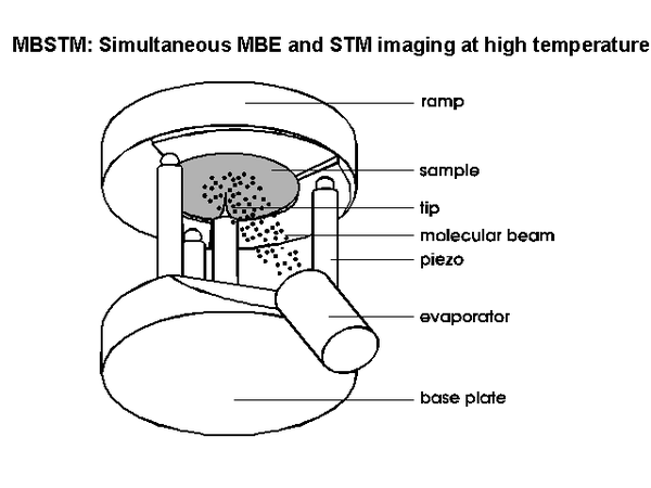
We used a beetle type STM with ramps for coarse approach . The sample holder which rests on the outer piezos consists of three ramps (see figure). Sample approach and xy-movement is done by inertial motion of the sample holder by the three outer piezos. Scanning is done by the centre piezo which holds the tip. All piezos are surrounded by a shield for high temperature operation and to prevent evaporation onto the piezos. The silicon sample is heated by direct current and the sample bias voltage is corrected for the voltage drop due to resistive heating. The thermal drift is considerable when the sample temperature is raised. After one hour at a fixed temperature (600-900K) the thermal drift decreases to ~30 Angström/min. During scanning we can correct for thermal drift. In successive images the same feature is marked and correction voltages are applied to the xy-scan signals to image the same surface area in successive images. The Ge evaporator is located under an angle of 50o from the sample normal. Due to the open design of the STM the molecular beam can be directed towards the sample which is located in the STM position. Part of the MBE beam impinging on the sample is shaded by the tip. With a typical tip radius of some hundred Å we use scan ranges of several thousand Å to minimise the fraction shaded by the tip.
Details can be found in:
Applied Physics Letters 63 (1993) 3055, and: Review of Scientific Instruments 67 (1996) 2568.