Assembly of van der Waals Heterostructures
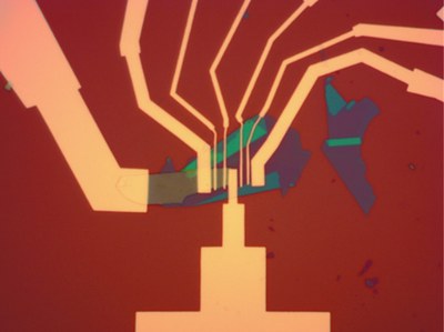
In our lab, we assemble heterostructures from exfoliated flakes of layered materials using novel polymer-based fabrication techniques, allowing the manipulation of flakes with micron precision, while maintaining atomically clean surfaces and interfaces.
Van der Waals (vdW) materials have a layered crystal structure consisting of atomically thin sheets with strong chemical bonds inside the plane, but weakly coupled to neighbouring layers. The resulting 2D nature of the sheets often gives rise to unique properties, especially when a single layer is isolated, making vdW materials not only interesting for fundamental research, but also applications. Since the discovery of graphene, many other vdW materials with a wide range of properties have been synthesised − from insulating to superconducting and magnetic. Due to the weak interlayer coupling, we can isolate atomically thin layers of vdW materials and manipulate them in a controlled way. We continuously advance our heterostructure fabrication techniques and have recently developed a ‘dry-transfer flip method’ which allows a complete in-situ preparation of heterostructures from air-sensitive materials while maintaining atomically clean surfaces. Using this technique, we are able to combine materials with different properties to engineer heterostructure properties via proximity effects, e.g., to realise topological superconductivity [1].
Furthermore, we investigate how a controlled mismatch of the atomic lattices in two or more layers, e.g., via rotational misalignment, gives rise to moiré effects which can alter the electronic properties of the materials altogether [2, 3] (see also our work on twisted graphene interfaces).