Loading
Novel Approach for Mechanical Assembly of Van-der-Waals Heterostructures
TO-194 • PT 1.3046 • As of 01/2024
Peter Grünberg Institute
Quantum Nanoscience (PGI-3)
Technology
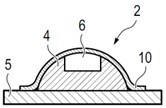
Our new invention represents a novel approach for the mechanical construction of van der Waals heterostructures. The method comprises the use of two polymer stamps, each with a recess in their center, on which polymer films are arranged such that they cover half of each recess, respectively. Using the stamps, van der Waals heterostructures are built up through sequential pick up of 2D materials by contacting their surfaces with the polymer stamps. Lastly, the heterostructure is put down and the polymer film is peeled off, leaving minimal residue on the heterostructure. The process offers the advantage that no cleaning methods, such as solvents or AFM cleaning, are required and it is compatible with protective atmospheres and vacuum environments. As a result, atomically clean heterostructures can be achieved at low process temperatures.
Problem addressed
Conventional Van der Waals heterostructures building techniques, such as the widely used "deterministic dry pick-up assembly" method, while versatile and capable of producing high-quality heterostructures, often leaves polymer residues on the heterostructure surface. This requires additional cleaning steps and can be problematic when the surface is reactive. One solution is to use a protective layer between the polymer and the reactive material, however, this limits accessibility. Another alternative is the "dry transfer-flip" technique, which involves building the heterostructure in reverse order and then flipping it upside down and removing polymer residue by baking in vacuum. However, heating heterostructures can cause atomic defects and is not compatible with 2D materials that decompose at elevated temperatures. These limitations highlight the need for a solution that provides a cleaner and more efficient alternative for building such heterostructures.
Solution
The key feature of our polymer stamps approach is that it allows to assemble heterostructures without directly touching them. To achieve this, at first, a handle flake is picked up with the polymer stamp, typically a large graphite flake. Using this handle, the remaining heterostructure is assembled. After that, the handle flake with the heterostructure on it is passed to the second stamp, and put down onto a sample substrate, flipping the heterostructure upside down in the process. As a result, the heterostructure surface is pointing upwards and has never been in contact with any polymers, solvents or air during the fabrication process. To achieve this, we use special polymer films on the stamps to facilitate the handling of the heterostructures during the assembly process. Our approach offers several advantages over conventional approaches. Firstly, the heterostructure interface and surfaces are extremely clean, such that they do not require any subsequent cleaning. This ultimately allows for the creation of heterostructures made from reactive materials with atomically clean surfaces and at relatively low process temperatures. Furthermore, the method provides deterministic assembly and placement of the heterostructures on the final substrate. As such, the method allows for the assembly of a wide range of material combinations, making it versatile and adaptable to different research and industrial applications.
Benefits and Potential Use
Our approach has various potential applications in the field of materials science and nanotechnology in, both, research and industry settings. The technology enables the precise assembly of van der Waals heterostructures, which are known for their unique electronic and optical properties. As a result, heterostructures are promising for applications in advanced electronic devices, such as transistors, sensors, and photovoltaic cells. The ability to create atomically clean interfaces between different materials opens up possibilities for studying fundamental physical phenomena and exploring new device functionalities. The method can also be applied in the fabrication of flexible and transparent electronics, as well as in the integration of 2D materials into existing semiconductor technologies, such as photovoltaics.
Development Status and Next Steps
Forschungszentrum Jülich has an extensive track record in the field of solid-state physics applications and holds several related patents. The device fabrication capabilities resulting from the invention have been demonstrated, and the technology described above is continuously being developed further. Forschungszentrum Jülich focuses on energy and cost-efficient devices, suitable for various emerging technologies. The Peter Grünberg Institute (PGI-3) – Quantum Nanoscience – in particular cooperates with numerous national and international companies and scientific partners who have potential applications of the novel approach.
TRL
4
Keywords
van der Waals heterostructures, 2D materials, polymers films, stamping, dry transfer, deterministic assembly
Contact us
Loading
More technologies
Loading
Last Modified: 02.06.2025