December 30, 1969
Loading
TO-129 • PT 1.3021 • As of 10/2023
Peter Grünberg Institute
Semiconductor Nanoelectronics (PGI-9)
Electronic components typically consist of layers or regions of semiconductor materials, part of which are doped to alter their electrical conductivity. Doping involves introducing small amounts of foreign atoms into specific areas of the semiconductor to manipulate its conductivity, creating electrical contacts or isolating regions. Conventionally, this process is carried out ex-situ after semiconductor growth has been completed. It requires the use of masks to selectively cover areas, resulting in additional fabrication steps, increased production time and complexity and a possible cause for material defects. Our approach offers an improved solution by depositing materials on pre-structured substrates, taking advantage of geometrical constraints and the fact that growth of compound semiconductors occurs only where the individual elements converge. This approach enables doping of selective areas already during the semiconductor epitaxy, streamlining the manufacturing process and reducing the number of ex-situ device fabrication steps. Therefore, our technology presents a promising alternative for potential licensees seeking more efficient and simplified production of electronic and optoelectronic components.
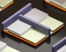
Conventional manufacturing processes of electronic components, such as field effect transistors or diodes, are facing several challenges. One of the main issues is the demanding requirement to selectively deposit different materials, semiconductors, oxides and metals, on a substrate. This hinders the production of complex electronic devices with specific functionalities. The required deposition, structuring and removal of masks for the selective epitaxy complicates the fabrication process and increases the risk of damaging the delicate structures. So, there is a need to address these issues and provide better solutions for the production of next generation electronic devices.
Our novel technology offers significant advantages over the previous state of the art. Firstly, it enables the selective deposition of different materials on a substrate, without any intermediate steps for preparation of dielectric masks. The selective deposition is achieved by using walls that shield specific areas of the substrate, ensuring that only the desired material is deposited in the intended regions. This streamlines the manufacturing process, reduces the risk of damage, and saves valuable time. Secondly, the new technology avoids the necessity for additional surface preparation steps prior each material deposition step. Since film growth can be performed using the very same mask, high quality interfaces between different materials can be expected without additional surface cleaning steps. This potentially allows for the creation of complex electronic and optoelectronic components with improved performance.
The new technology offers a simplified fabrication of a wide range of applications in the electronics industry. It can be adapted to the production of various electronic components such as transistors, diodes, and integrated circuits. The ability to selectively deposit different materials, including the selective doping of different compound semiconductor device regions, facilitates the in-situ fabrication of complicated device structures and improves their performance and functionality. In addition, precise control of material deposition opens up opportunities for the development of novel devices and technologies, including sensors, photovoltaics, and optoelectronic devices.
Forschungszentrum Jülich has extensive expertise in this field and holds several patents. The technology described above has already been initially verified through prototypes and is continuously being developed further. The Peter Grünberg Institute (PGI-9) – Semiconductor Nanoelectronics – already cooperates with numerous national and international companies and scientific partners. Forschungszentrum Jülich focuses on energy and cost-efficient devices, suitable for various emerging technologies. We are continuously seeking for cooperation partners and/or licensees in this and adjacent areas of research and applications.
TRL
4
Keywords
Compound semiconductor, semiconductor layers, material deposition, shadow mask, CMOS