Advanced Approach for Creating Ohmic Contacts in “Buried Channel” III-V / II-VI Compound Semiconductors
TO-125 • PT 1.2853 • As of 10/2023
Peter Grünberg Institute
Semiconductor Nanoelectronics (PGI-9)
Technology

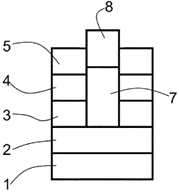
Our new approach aims to create an ohmic contact for electronic components, specifically for internal (so-called “buried channel”) III-V or II-VI compound semiconductors, suitable for operation at low temperatures in quantum technology. We thus propose to apply a semiconductor layer (2) to a specific substrate (Figure 1) (1). The surface of this semiconductor layer (2) is chemically etched, rinsed with radicals, and allows to deposit an electrical conductor (8) on top of a semiconductor (7) on the rinsed surface of the semiconductor (2). This process creates a low-resistance connection to the semiconductor layer (2) which would be susceptible to damage in case of conventional manufacturing methods. Our approach specifically describes an electronic component that includes multiple semiconductor layers (2, 3, 4) which consist of different adjacent II-VI semiconductors on the substrate (1). These layers are covered by a non-conductive dielectric layer (5). An entrance in the cover layer is partially filled with a II-VI semiconductor (7) and leads to one of the semiconductor layers. A metal contact (8) is applied onto this II-VI semiconductor (7), which extends beyond the cover layer (5). In this way, the electrical conductor (8) and the semiconductor (7) can form a conducting channel to the buried semiconductor layer (2).
Problem addressed
An ohmic contact is a low-resistance transition between a metal and a semiconductor. Current manufacturing techniques for those ohmic contacts in electronic components are facing several challenges. One problem is creating a local ohmic contact for internal (so-called “buried channel”) semiconductors, which are semiconductors located inside electronic components. Another issue is the difficulty in achieving high-grade ohmic contacts for compound semiconductors, such as ll‑VI and Ill-V compounds.
High temperatures required for metal alloying is likely to damage the crystal structure of these semiconductors, leading to reduced conductivity. Additionally, ion implantation, a common technique for introducing dopants in order to contact a buried channel, are likely to harm the crystal structure. These limitations hinder the operation of efficient ohmic contacts at low temperatures, which is crucial for emerging quantum technologies like spin qubits.
Solution
Our new technology offers several advantages. By chemically etching and rinsing the semiconductor surface in an ultrahigh vacuum with hydrogen radicals at elevated temperature, we can overcome the challenges associated with creating low-resistance contacts in sensitive III‑V and II-VI compound semiconductors. This results in linear current-voltage characteristics and extremely low contact resistances at both room temperature and cryogenic temperatures.
Benefits and Potential Use
The new technology has various applications in electronic devices. It enables the creation of ohmic contacts for buried transport channels in semiconductors, making it suitable for manufacturing unipolar devices such as 2D or 3D field-effect transistors or electrostatically defined electron spin qubits. The method can be used to fill holes in the dielectric layer with doped semiconductors, allowing for the integration of gate electrodes. The technology is particularly beneficial for creating high-quality contacts in compound semiconductors used in quantum computing applications. Overall, our technology offers improved contact properties and opens up new possibilities for the development of advanced electronic components.
Development Status and Next Steps
Forschungszentrum Jülich has extensive expertise in this field and holds several patents. The technology described above has already been initially verified through prototypes and is continuously being developed further.
The Peter Grünberg Institute (PGI-9) – Semiconductor Nanoelectronics – already cooperates with numerous national and international companies and scientific partners. Forschungszentrum Jülich focuses on energy and cost-efficient devices, suitable for various emerging technologies. We are continuously seeking for cooperation partners and/or licensees in this and adjacent areas of research and applications.
TRL
4️
IP
PCT/EP2020/059394, DE102019205376, EP3956923, WO2020212154, US20220216306, JP2022529927, CN113692642
Keywords
Ohmic contact, spin qubits, semiconductor layers, II-VI semiconductors, III-V semiconductors
