Solar TAP
Printed solar cells that are environmentally friendly and flexible are also the focus of the Solar TAP innovation platform, which Christoph Brabec is helping to coordinate.
Roll-up displays and photovoltaic films for façades – organic electronics have a great deal of potential. However, recycling concepts should be in place before the new technology becomes a mass product, recommends materials researcher Christoph Brabec.
Mr. Brabec, together with colleagues from Germany, the UK, and the USA, you have called for the sustainable development of organic electronics. Could you tell us a bit more about this?
The technology is being used in more and more products. Displays are currently the largest market – known as AMOLED or OLED for TVs and smartphones. And more applications are set to be added. To avoid producing unnecessary electronic waste in future, we need to design sustainable solutions today – for example for production and recycling. In 20 years’ time, when a mass market may have developed, it will be too late.
What does organic electronics refer to exactly?
This is a collective term for electronic circuits consisting of organic polymers or smaller organic molecules. Above all, it refers to semiconductors, which are the central building blocks of all digital devices. Conventional variants are largely based on silicon, while the organic ones are mainly based on carbon.
What is the difference between silicon and carbon semiconductors?
In contrast to silicon, which is grown as a single crystal, the organic compounds are chemically synthesized. Organic electronics can be produced in a relatively energy-efficient manner in comparison and the process is well suited to producing large-format, thin electronic layers – such as flexible polymer films. Organic electronics also offer advantages for photovoltaics.

To avoid producing unnecessary electronic waste in future, we need to design sustainable solutions for organic electronics today. In other words, we not only need to develop manufacturing processes and properties, but also plan for technical recycling solutions in the laboratory. In 20 years’ time, when a mass market may have developed, it will be too late.
What are these advantages?
Organic semiconductors are very easy to make transparent. They then absorb infrared light, i.e. thermal radiation, but not visible light. Unlike conventional silicon semiconductors, they can still achieve high performance efficiency despite being so thin. This makes them particularly suitable for integrated PV systems in façades, windows, or photovoltaics above agricultural land, for example. Another emerging market is devices connected to the Internet of Things, such as small electronic gadgets and sensors that can be operated without batteries.
And what about the environmental impact?
If you look at the entire value chain for solar cells, organic-based semiconductors release two to three times less CO2 than silicon-based ones. The production process involves low energy consumption and the low weight of the films makes the technology particularly suitable for transportation and assembly. You end up with significantly more watts per gram.
But organic electronics are still relatively expensive?
Yes, that’s because there are millions of different organic semiconductors. In practice, no standard material has yet become established and no value chain has been consolidated. This makes production expensive. But we assume that this will change. It is therefore important to look at the entire life cycle of the components today in order to minimize the ecological footprint.
So what needs to be done?
Many electronic components are difficult to take apart again. Organic electronics should be designed so that they can be easily and economically recycled. The energy and costs involved in recycling must not be higher than for production. We have to take this into account right from the development stage. The goal is to establish a circular economy.
Tailored properties
Conventional semiconductors have an ordered crystalline or polycrystalline structure, whereas the organic variants are disordered. This is due to the manufacturing process, in which the organic polymers are initially present in solution. When evaporating on a surface, the molecules arrange themselves in an irregular pattern; experts also speak of an amorphous microstructure. But even here, certain recurring areas with ordered structures, known as domains, are formed. Depending on the size and characteristics of these domains, the organic semiconductor structures can therefore have completely different properties. With the support of AI, Jülich scientists are researching the influence of production on the end result in an attempt to tailor certain properties.
And how can that be achieved?
Through multi-layer designs, for instance, with components consisting of easily separable layers. It is thus possible to ensure that various materials can be easily recycled at the end of their product life. Organic semiconductors are very well suited for this because they can be easily dissolved again in contrast to silicon-based semiconductors. We should also use easily recyclable or easily degradable substrates and ensure that no toxic substances are used in production.
How is your research making a contribution?
At our institute, we are focused on manufacturing processes. We investigate the influence of production on the end result – in other words a finished organic semiconductor – and we also try to optimize the process so that the semiconductor delivers the best possible performance.
How do you go about this?
We build research and development facilities that are controlled by artificial intelligence. The AI helps us to find the “simplest” but most suitable materials and to optimize their manufacturing process – for example, materials for organic solar cells that are high-performance, long-lasting, and easy to recycle. We thus want to make renewable energy even more sustainable and more attractive in the future.
Personal background
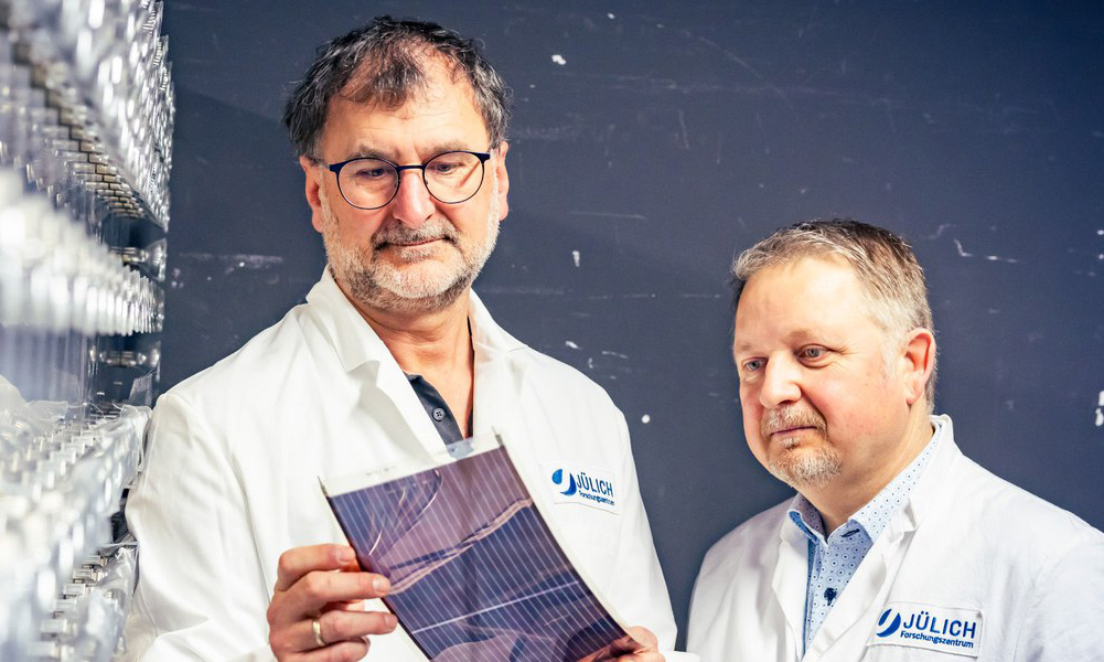
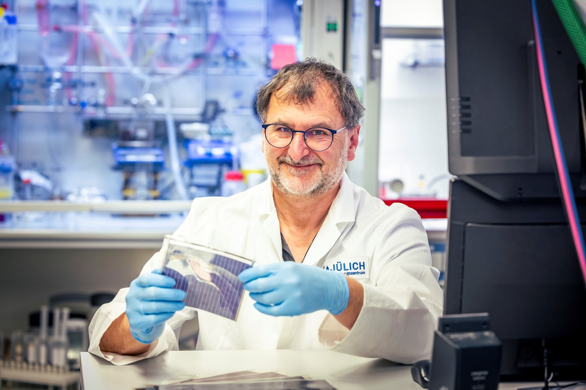
Prof. Christoph Brabec is a director at the Helmholtz Institute Erlangen-Nürnberg for Renewable Energy (IET-2), a branch office of Forschungszentrum Jülich. At IET-2, he heads the research department High-Throughput Methods in Photovoltaics. At the same time, he holds the Chair of Materials for Electronics and Energy Technology at Friedrich-Alexander Universität Erlangen-Nürnberg. The materials researcher regularly appears in the list of the world’s most highly cited researchers.
The interview was conducted by Janosch Deeg, pictures Martin Leclaire and @EnCN.